Wafer and Substrate Selection Guide for Optoelectronics and Photonics Applications
In optoelectronics and photonics, the performance and reliability of devices such as LEDs, lasers, photodetectors, and modulators depend significantly on the choice of wafer and substrate materials. The right substrate not only supports the active layers physically but also ensures lattice matching, thermal conductivity, and electrical isolation, which are critical for efficient device operation. As materials science advances, manufacturers must navigate a complex array of substrate options, each with unique properties tailored to specific applications.
This article offers a comprehensive comparison of wafer and substrate materials commonly used in optoelectronic and photonic applications, with a focus on their structural, thermal, and electrical properties, backed by recent data and references.
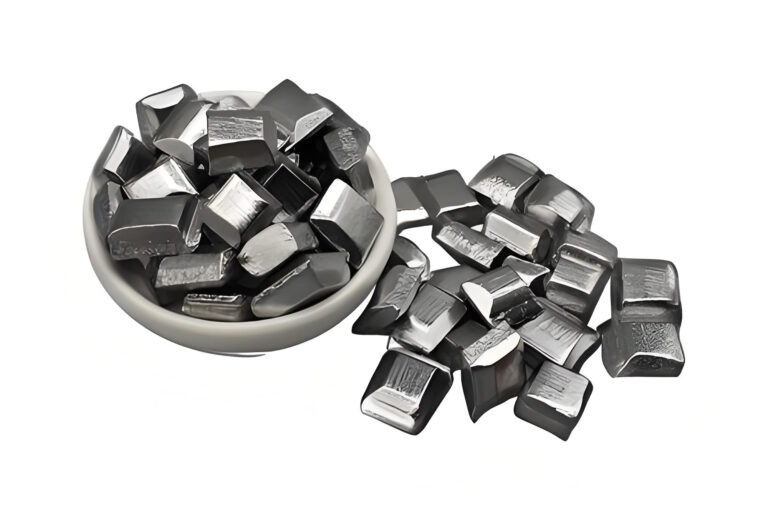
1. Silicon (Si) Wafers
Silicon is the most widely used substrate in electronics due to its low cost, well-developed processing techniques, and excellent mechanical properties. However, in optoelectronics, its indirect bandgap limits its application in light-emitting devices.
Reference: Sze, S. M., & Ng, K. K. (2006). Physics of Semiconductor Devices. Wiley.
2. Sapphire (Al₂O₃) Substrates
Sapphire is a preferred substrate for GaN-based LEDs and RFICs due to its high thermal stability, electrical insulation, and transparency in the visible and UV spectrum.
Reference: Liu, Y., et al. (2019). “Thermal and Optical Properties of Sapphire Substrates for High-Power LEDs,” Optical Materials, 94, 206-210.
3. Gallium Arsenide (GaAs) Wafers
GaAs offers a direct bandgap and high electron mobility, making it ideal for high-frequency and optoelectronic devices such as laser diodes and solar cells.
Reference: Jain, S. C., et al. (1996). “III–V compound semiconductor electronic devices,” Solid-State Electronics, 40(5), 629-647.
4. Silicon Carbide (SiC) Substrates
SiC substrates are known for their high thermal conductivity, chemical stability, and wide bandgap, making them suitable for power electronics and UV photonic devices.
Reference: Kimoto, T., & Cooper, J. A. (2014). Fundamentals of Silicon Carbide Technology. Wiley.
5. Gallium Nitride (GaN) on Substrate
While free-standing GaN substrates are expensive, GaN is commonly grown on foreign substrates such as sapphire, SiC, or Si using epitaxial techniques.
Reference: Ponce, F. A., & Bour, D. P. (1997). “Nitride-based semiconductors for blue and green light-emitting devices,” Nature, 386(6623), 351–359.
6. Indium Phosphide (InP) Wafers
InP provides a direct bandgap with high electron velocity, widely used in photonic integrated circuits (PICs) and high-frequency devices.
Reference: Coldren, L. A., et al. (2012). Diode Lasers and Photonic Integrated Circuits. Wiley.
Substrate Selection Considerations
| Material | Bandgap (eV) | Thermal Conductivity (W/m·K) | Lattice Constant (Å) | Transparency | Application Domain |
|---|---|---|---|---|---|
| Si | 1.12 | 149 | 5.43 | No | Photonics, solar |
| Sapphire | 8.8 | 25 | 4.76 | Yes | LEDs, RF, optics |
| GaAs | 1.42 | 55 | 5.65 | Partial | Lasers, RF, PV |
| SiC | 3.26 | 490 | 3.07 | Partial | Power, UV optics |
| GaN (on SiC) | 3.4 | — | ~3.2 | Yes | LEDs, HEMTs |
| InP | 1.34 | 68 | 5.87 | Partial | Lasers, high-speed PICs |
Selecting the appropriate wafer or substrate is critical in determining device efficiency, yield, and cost-effectiveness in optoelectronics and photonics. While silicon remains ubiquitous, materials such as sapphire, GaAs, SiC, GaN, and InP enable specific functionalities in advanced applications. As device demands grow more complex, substrate engineering will continue to be a cornerstone of innovation.