Showing 13–24 of 40 results
-
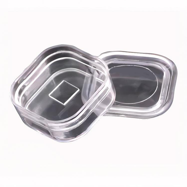
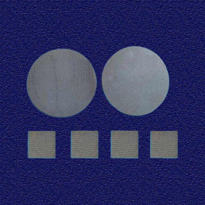
 – 001 Orientation, 10 × 10 × 0.5 mm")
$1,285.00
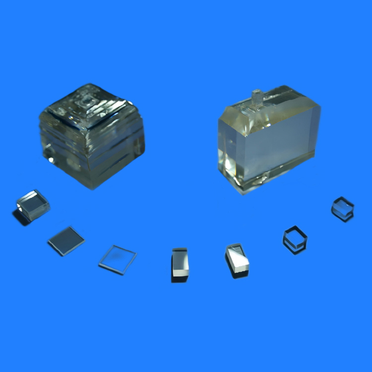
- Single crystal KTN with composition KTa₀.₅Nb₀.₅O₃
- <001> crystallographic orientation for optimal electro-optic performance
- Size: 10 × 10 × 0.5 mm
- High electro-optic coefficient (r33 ≈ 30–50 pm/V)
- Strong photorefractive effect
- Excellent dielectric tunability
- Wide optical transparency (~350 nm – 5500 nm)
- Low defect density and high optical uniformity
-
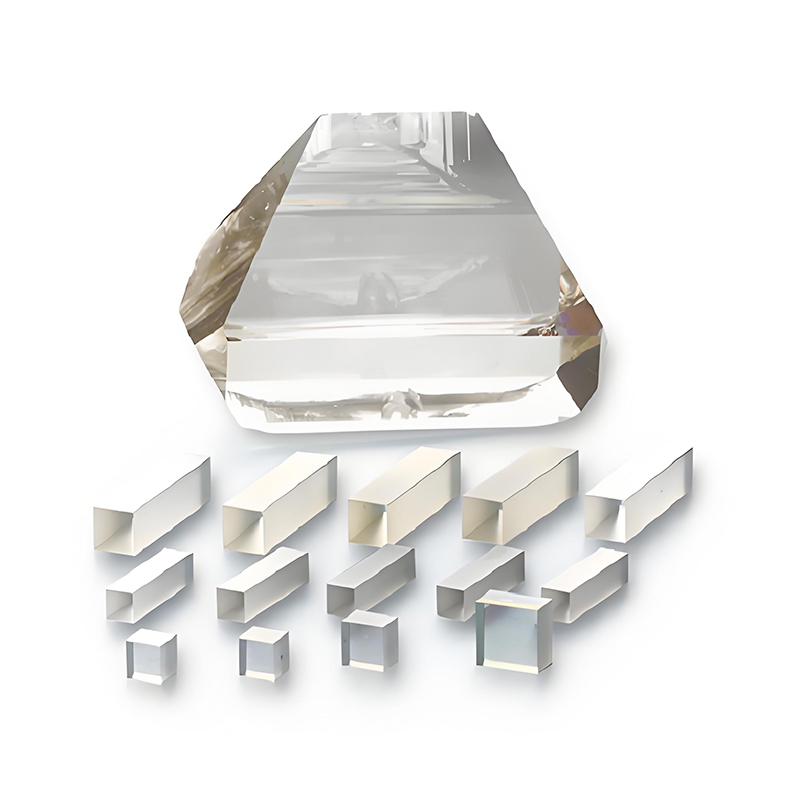

- High Nonlinear Optical Coefficient: ~15 times that of KDP crystals.
- Broad Transparency Range: 350 nm to 4500 nm.
- High Damage Threshold: >500 MW/cm² for nanosecond pulses.
- Excellent Electro-optic Properties: Suitable for Q-switching and Pockels cells.
- Large Angular Acceptance and Low Walk-off Angle: Easier beam alignment and higher conversion efficiency.
- Stable Physical and Chemical Properties: High mechanical strength and environmental stability.
-

- Excellent Crystal Quality: Low dislocation density, high structural perfection.
- Ideal Lattice Match: Close lattice parameters with materials like YBCO, LSMO, PZT, and other perovskite oxides.
- High Thermal Stability: Suitable for high-temperature thin film deposition processes.
- High Dielectric Constant: Beneficial for microwave devices and tunable capacitors.
- Low Dielectric Loss: Ensures superior performance at high frequencies.
- Chemical Stability: Strong resistance to acids and bases.
- Atomically Smooth Surface: Achieved through advanced polishing and chemical etching processes.
-

- High Thermal Stability: Excellent performance under high temperatures up to 1500°C.
- Wide Bandgap: Enables use in deep UV and high-power electronic applications.
- Superior Mechanical Strength: Resists thermal shock and mechanical stress.
- Excellent Lattice Match: Ideal substrate for GaN, AlN, ZnO, and other oxide semiconductor epitaxial growth.
- Low Dielectric Loss: Beneficial for microwave and RF device applications.
- Chemical Inertness: High resistance to acids, alkalis, and environmental degradation.
- Smooth, Defect-Free Surface: Essential for high-yield epitaxial growth and thin-film deposition.
-

- Wide Transmission Range: Excellent optical transmission from 120 nm (VUV) to 6 μm (IR).
- Low Refractive Index: ~1.39 at 400 nm, advantageous for minimal Fresnel losses.
- Radiation Resistance: High durability against X-rays and high-energy particle irradiation.
- High Optical Homogeneity: Suitable for precision optics and laser systems.
- Good Mechanical Properties: Higher hardness compared to other VUV transparent materials like CaF₂.
- Low Birefringence: Enabling better performance in polarization-sensitive applications.
- Chemical Stability: Moderate chemical inertness; surface can be protected with appropriate coatings if needed.
-
 – Tinsan Materials")
- High Electro-optic Coefficient: Enables efficient light modulation
- Excellent Nonlinear Optical Properties: Ideal for frequency conversion processes
- Wide Transmission Range: Suitable for UV, visible, and infrared applications
- Strong Piezoelectric Response: Essential for SAW and MEMS devices
- Photorefractive Effect: Useful for holography and optical data storage
- Chemical and Thermal Stability: High reliability in demanding environments
- Availability of Stoichiometric and MgO-doped Variants: Reduces photorefractive damage and enhances performance in high-power lasers
- Precise Crystal Growth and Wafer Fabrication: Ensures high uniformity and low defect densities
-

- Wide Transparency Range: 160 nm to 2600 nm
- Broad Phase-Matching Capability: Suitable for SHG, THG, OPO, SFG, DFG across UV to IR
- High Damage Threshold: >2 GW/cm² for 1064 nm, 10 ns pulse
- Low Walk-Off Angle: Ideal for high-beam-quality laser systems
- High Nonlinear Coefficients: Enables efficient frequency conversion
- Excellent Optical Homogeneity: Δn < 10⁻⁶/cm
- Good Mechanical Hardness: Mohs hardness ~6
- Stable Physical and Chemical Properties: Resistant to humidity and environmental degradation
- Nonhygroscopic: No special humidity control required
-
 Single Crystal Substrate – Tinsan Materials")
- Excellent Lattice Matching: Ideal match for many perovskite oxides such as YBCO, BST, and PZT
- High Thermal Stability: Maintains structural integrity under high temperatures
- Low Dielectric Loss: Suitable for microwave and dielectric applications
- High Crystallinity: Enables defect-free epitaxial film growth
- Good Mechanical Strength: Durable for various thin-film deposition processes
- Smooth Surface Finish: Atomic-level flatness for epitaxial growth
- High Chemical Stability: Resists degradation during processing
- Wide Application Range: Compatible with superconducting, ferroelectric, and oxide-based systems
-

- Lightest Structural Metal: Exceptionally low density for weight-sensitive applications
- Excellent Specific Strength: High strength-to-weight ratio
- Anisotropic Mechanical Properties: Ideal for deformation and slip system studies
- High Ductility at Elevated Temperatures: Improved formability in warm/hot conditions
- Good Machinability: Easier to process compared to other metals
- High Thermal Conductivity: Facilitates efficient heat dissipation
- Superior Homogeneity: Enables reproducible experimental results
- Corrosion Sensitivity: Useful for corrosion research and protective coating studies
-

- Excellent Thermal Stability: Suitable for high-temperature processing (melting point ~2135°C)
- Wide Optical Transmission: From 200 nm (UV) to 5000 nm (Mid-IR)
- Superior Mechanical Strength: High hardness and fracture toughness
- Low Thermal Expansion: 8.5 × 10⁻⁶ /°C at 25°C
- High Chemical Resistance: Stable in both acidic and alkaline environments
- Low Dielectric Loss: Favorable for microwave and RF applications
- Surface Quality: Polished to atomic-level smoothness (Ra < 5 Å)
- High Purity: Low levels of impurities ensuring consistent and repeatable results
-
 Single Crystal Substrates – Tinsan Materials")
- Excellent lattice matching for oxide thin films
- Wide transparency from UV to IR regions (0.3μm–6μm)
- High thermal conductivity and melting point (2852°C)
- Chemically inert to most acids and alkalis
- Low dielectric constant (ε ≈ 9.65 at 1MHz)
-
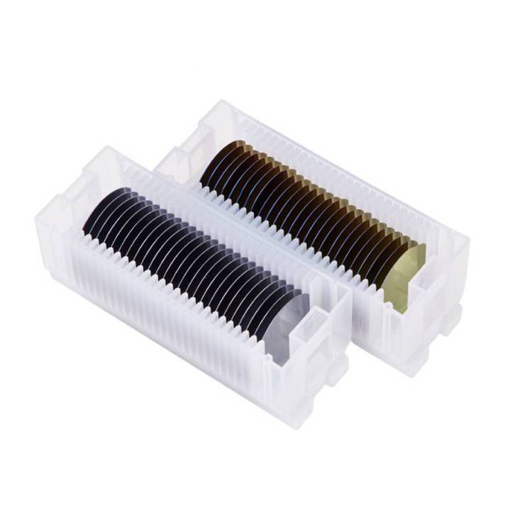

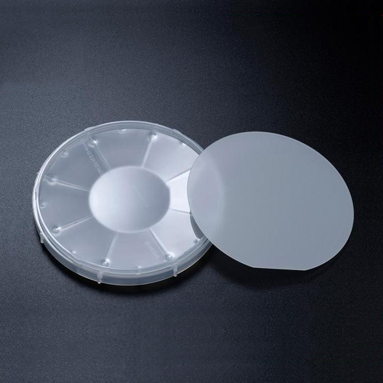
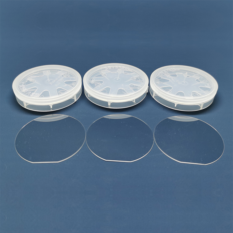
- Diameter Choices: 2″ to 12″ (or custom sizes).
- Doping Concentration: Custom doping profiles for N-type and P-type wafers.
- Thickness Variability: From ultra-thin wafers to thick substrates.
- Crystal Orientation: Standard orientations include <100>, <111>, <110>, with custom orientations available.
- Flat & Edge Treatment: Rounded, chamfered, or custom edge profiles.
- Surface Finishing:
- SSP (Single-Side Polished) or DSP (Double-Side Polished).
- Oxide coating, etched surfaces, or epitaxial layers upon request.