Aluminum Nitride (AlN) Single Crystal Substrates
- Ultra-High Thermal Conductivity: Up to 285 W/m·K, comparable to diamond.
- Wide Bandgap: ~6.2 eV, ideal for UV optoelectronic devices.
- High Electrical Resistivity: Excellent insulation properties.
- Superior Chemical and Thermal Stability: Suitable for harsh environments.
- Low Dielectric Constant and Loss: Enables high-frequency applications.
- High Mechanical Strength and Hardness: Durable under mechanical stress.
- Perfect Lattice Match for GaN: Supports high-quality epitaxial GaN growth.
Custom products or bulk orders, please contact us for competitive pricing!
- Satisfaction Guaranteed
- No Hassle Refunds
- Secure Payments
Description
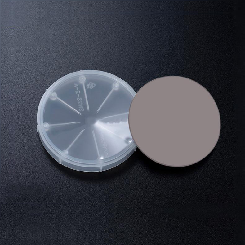
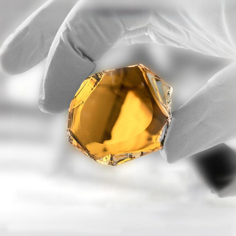
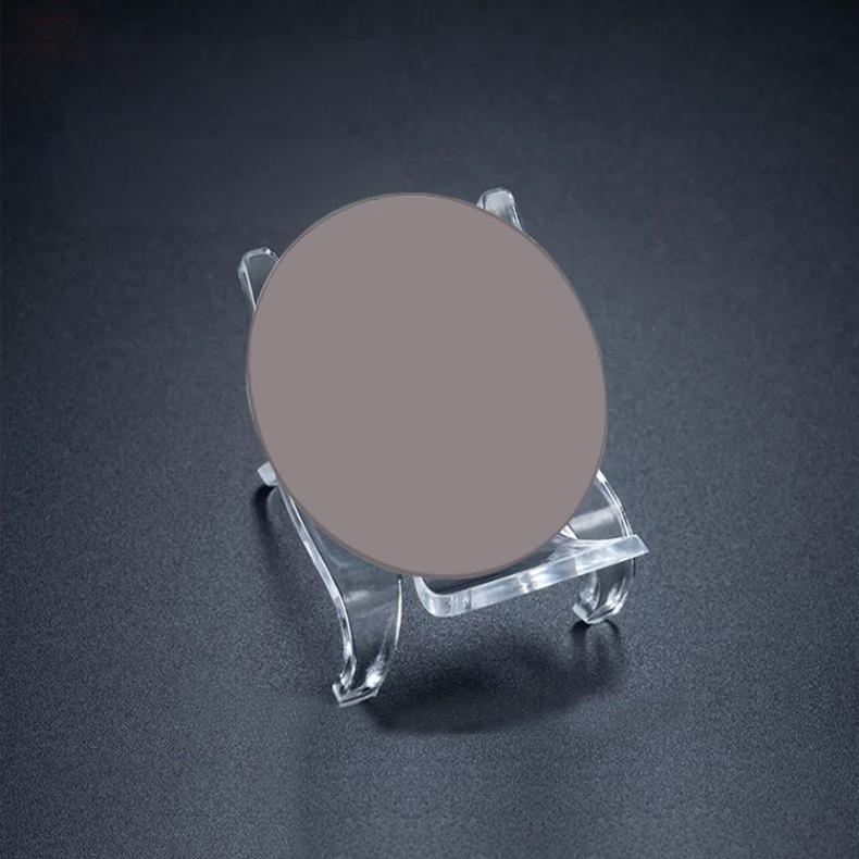
Aluminum Nitride (AlN) single crystal substrates are highly valued for their outstanding thermal conductivity, excellent electrical insulation, wide bandgap, and high-temperature stability.
These properties make AlN substrates ideal for high-frequency, high-power electronic devices, UV optoelectronic components, and advanced semiconductor applications.
We provide premium-quality AlN single crystal substrates with customizable sizes, orientations, and surface finishes to meet the stringent demands of next-generation technologies.
Crystal Structure and Orientation:
- Chemical Formula: AlN
- Crystal Structure: Hexagonal wurtzite (similar to GaN)
- Space Group: P6₃mc
- Lattice Constants:
- a = 3.112 Å
- c = 4.982 Å
- Density: ~3.26 g/cm³
- Melting Point: ~2200°C
- Thermal Expansion Coefficient:
- a-axis: 4.2 × 10⁻⁶/K
- c-axis: 5.3 × 10⁻⁶/K
- Available Orientations:
- (0001) c-plane (polar)
- (10-10) m-plane (non-polar)
- (11-20) a-plane (non-polar)
- Semi-polar orientations upon request
Key Properties and Advantages:
- Ultra-High Thermal Conductivity: Up to 285 W/m·K, comparable to diamond.
- Wide Bandgap: ~6.2 eV, ideal for UV optoelectronic devices.
- High Electrical Resistivity: Excellent insulation properties.
- Superior Chemical and Thermal Stability: Suitable for harsh environments.
- Low Dielectric Constant and Loss: Enables high-frequency applications.
- High Mechanical Strength and Hardness: Durable under mechanical stress.
- Perfect Lattice Match for GaN: Supports high-quality epitaxial GaN growth.
Typical Applications:
- Substrate for high-frequency and high-power GaN-based devices (HEMTs, LEDs)
- Deep ultraviolet (DUV) and UV-C light-emitting diodes
- Power electronics and RF devices
- Surface Acoustic Wave (SAW) and Bulk Acoustic Wave (BAW) filters
- Sensors operating in extreme environments (high temperature, corrosive)
- Photonic crystals and optoelectronic components
- Research and development of next-generation semiconductors
Specifications:
| Diameter | 10 mm – 50.8 mm (customizable) |
| Thickness | 0.3 mm – 1.0 mm |
| Orientation | (0001), (10-10), (11-20), custom available |
| Surface Finish | Double-side polished (DSP) or single-side polished (SSP) |
| Surface Roughness | ≤0.5 nm RMS (atomic scale polishing) |
| Surface Quality | 10-5, 20-10 Scratch-Dig per MIL-PRF-13830B |
| Dislocation Density | ≤10⁴ cm⁻² (high-quality) |
| Off-Cut Angle | On-axis or 0.1°-4° off-axis as specified |
| Growth Method | Physical Vapor Transport (PVT) Method |
Available Sizes and Customization:
- Sizes: 10 mm × 10 mm, 20 mm × 20 mm, 2-inch (50.8 mm), custom
- Thickness Options: 0.3 mm, 0.5 mm, 1.0 mm, or customized
- Polishing Options:
- Double-side polished (DSP) for epitaxial applications
- Single-side polished (SSP) for other purposes
- Orientation Tolerance: ±0.5° or better
- Edge Finish: Chamfered or beveled edges for safe handling
- Surface Flatness: ≤5 μm Bow/Warp available
- Special Options:
- Low-defect density substrates
- Customized off-axis cuts for specific device fabrication needs
Quality Assurance:
We guarantee exceptional quality through:
- High-Resolution X-ray Diffraction (HRXRD) for crystal quality analysis
- Laue back-reflection and XRD mapping to verify orientation and uniformity
- Atomic Force Microscopy (AFM) for surface roughness measurement
- Defect inspection (TDD, micropipes, stacking faults) using advanced methods
- Surface flatness, thickness, and dimension inspection
- Class 1000 cleanroom packaging for ultra-clean delivery
Why Choose Our AlN Single Crystal Substrates?
- Ultra-high thermal conductivity for efficient heat dissipation
- Wide bandgap for UV optoelectronic and high-power device applications
- Ultra-smooth surfaces optimized for epitaxial growth
- Industry-leading quality with customizable specifications
- Strong technical support for application-specific solutions
- Fast turnaround times and global shipping service
Ordering & Contact Information:
Tinsan Materials offers flexible MOQ (Minimum Order Quantity) and competitive pricing. Our substrates are packaged in Class 100 cleanroom environments and shipped worldwide. For custom orders or technical inquiries, please contact us for a detailed consultation!
