Single Crystal Substrates - Tinsan Materials")

 Single Crystal Substrate - Tinsan Materials")
Barium Fluoride (BaF2) Single Crystal Substrates
- Ultra-Wide Transmission Range (DUV to IR): 150 nm to 12–15 μm.
- Low Refractive Index: Minimizes reflection losses without extensive coatings.
- High Radiation Resistance: Suitable for high-radiation environments such as space and nuclear detectors.
- Low Dispersion: Excellent for optical systems requiring minimal chromatic aberration.
- Good Mechanical Properties: Higher fracture toughness compared to other fluoride crystals.
- Low Absorption and High Optical Quality: Especially critical in high-resolution spectroscopic systems.
- Compatibility with High-Energy Lasers: Due to high laser-induced damage threshold.
- Ease of Cleaving and Processing: Supports cost-effective manufacturing.
- Stable Physical and Chemical Properties: Good moisture resistance compared to other fluorides.
Custom products or bulk orders, please contact us for competitive pricing!
- Satisfaction Guaranteed
- No Hassle Refunds
- Secure Payments
Description
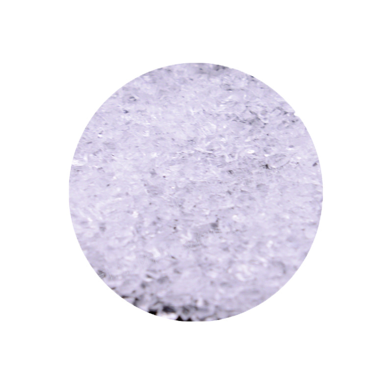
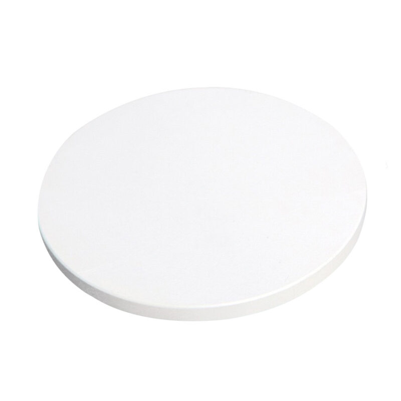
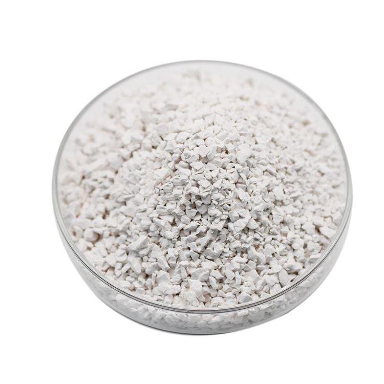
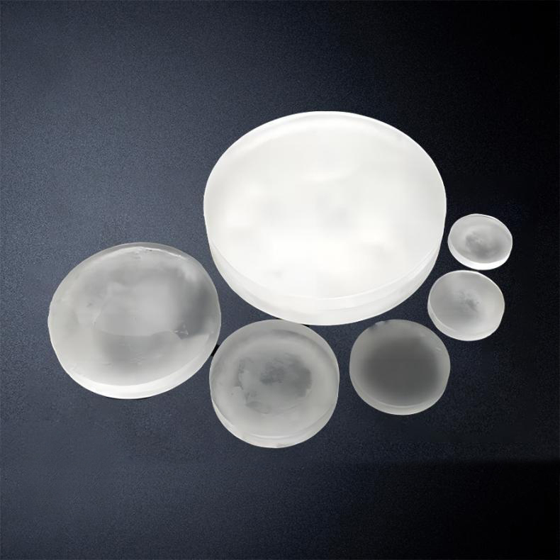
Barium Fluoride (BaF₂) single crystal substrates are valued for their broad optical transmission range extending from the deep ultraviolet (DUV) at around 150 nm to the infrared (IR) at approximately 12–15 µm. BaF₂ exhibits excellent transmission, low refractive index, high resistance to high-energy radiation, and good mechanical properties, making it a preferred material for infrared spectroscopy, ultraviolet optics, scintillation detectors, and space optics.
We offer high-purity BaF₂ single crystal wafers and substrates tailored to meet the most demanding requirements in optical, laser, and semiconductor fields.
Crystal Structure and Orientation:
- Chemical Formula: BaF₂
- Crystal System: Cubic (Fluorite structure)
- Lattice Constant: a = 6.200 Å
- Transparency Range: 0.15 μm to 12–15 μm
- Refractive Index: ~1.4749 at 589 nm
- Density: 4.89 g/cm³
- Hardness (Mohs): 3–4
- Melting Point: 1368°C
- Available Orientations:
- (100) Orientation: Standard for optical and epitaxial applications
- (111) Orientation: Offers specific optical characteristics
- (110) Orientation: Available for customized requirements
- Special or customized orientations available on request
Key Properties and Advantages:
- Ultra-Wide Transmission Range (DUV to IR): 150 nm to 12–15 μm.
- Low Refractive Index: Minimizes reflection losses without extensive coatings.
- High Radiation Resistance: Suitable for high-radiation environments such as space and nuclear detectors.
- Low Dispersion: Excellent for optical systems requiring minimal chromatic aberration.
- Good Mechanical Properties: Higher fracture toughness compared to other fluoride crystals.
- Low Absorption and High Optical Quality: Especially critical in high-resolution spectroscopic systems.
- Compatibility with High-Energy Lasers: Due to high laser-induced damage threshold.
- Ease of Cleaving and Processing: Supports cost-effective manufacturing.
- Stable Physical and Chemical Properties: Good moisture resistance compared to other fluorides.
Typical Applications:
- Optical components (windows, lenses, prisms) for DUV, UV, visible, and IR regions
- IR spectroscopy, FTIR instruments
- Space and aerospace optical systems
- High-energy particle detectors and scintillators
- Laser systems optics
- UV lithography optics
- Excimer laser optics
- X-ray detection systems
- Medical imaging and analytical equipment
- Photonic and semiconductor research fields
Specifications:
| Diameter | 10 mm – 100 mm (larger sizes available) |
| Thickness | 0.2 mm – 5 mm (custom options) |
| Orientation | <100>, <111>, <110>, custom |
| Surface Finish | Optical polish (10-5 Scratch-Dig or better) |
| Surface Flatness | λ/8 or better @ 632.8 nm |
| Parallelism | <10 arc seconds |
| Transmission | >90% across the transparency range |
| Surface Roughness (Ra) | <5 Å (Atomic Force Microscope measured) |
| Coating Options | Anti-Reflection (AR) coatings for UV/IR |
| Edge Treatment | Beveled or as-cut options |
Available Sizes and Customization:
- Wafer Sizes: 10 mm, 20 mm, 25 mm, 50.8 mm (2 inch), 76.2 mm (3 inch), 100 mm (4 inch), custom
- Thickness Options: 0.2 mm, 0.5 mm, 1 mm, 2 mm, others available
- Polishing Types:
- Single-Side Polished (SSP)
- Double-Side Polished (DSP)
- Orientation Accuracy: ±0.5° or higher precision on demand
- Special Treatments:
- Ultra-smooth optical polishing
- Ultra-clean vacuum packaging
- Customization: Sizes, thickness, orientations, polishing grade, surface roughness, and coatings can all be customized.
Quality Assurance:
All BaF₂ substrates are produced and inspected according to strict quality standards, including:
- X-ray Diffraction (XRD) for crystallographic quality verification
- Optical Transmission Spectrometry to confirm high transmittance
- Surface Interferometry for flatness evaluation
- Microscopic visual inspection for scratches, pits, and inclusions
- Measurement of thickness, parallelism, and surface quality
- Cleanroom packaging to prevent contamination
Why Choose Our Barium Fluoride (BaF₂) Substrates?
- Superior-quality BaF₂ crystals with high transmittance across the UV to IR range
- Custom substrate manufacturing based on your project needs
- Precision optical polishing and advanced surface finishing
- Rapid production and delivery with flexible order volumes
- Highly experienced technical support team
- Proven supply record to optics, aerospace, semiconductor, and photonics industries worldwide
Ordering & Contact Information:
We offer flexible MOQ (Minimum Order Quantity) and competitive pricing. Our substrates are packaged in Class 100 cleanroom environments and shipped worldwide. For custom orders or technical inquiries, please contact us for a detailed consultation!
 Single Crystal Substrates – Tinsan Materials")