 Single Crystal Substrates - Tinsan Materials")

 Single Crystal Substrate - Tinsan Materials")
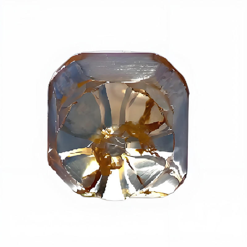
Barium Titanate (BaTiO3) Single Crystal Substrates
- Ferroelectric behavior with spontaneous polarization
- Extremely high dielectric constant (up to thousands near Curie temperature)
- Piezoelectric and electro-optic effects
- Cubic structure at high temperature, tetragonal below Curie temperature (~120°C)
- Suitable for integration with other perovskite materials
- Atomically smooth surfaces achievable for epitaxy
Custom products or bulk orders, please contact us for competitive pricing!
- Satisfaction Guaranteed
- No Hassle Refunds
- Secure Payments
Description
Barium Titanate (BaTiO₃, BTO) is a ferroelectric perovskite oxide crystal known for its high dielectric constant, spontaneous polarization, and excellent piezoelectric properties. As a substrate, it is widely used for the epitaxial growth of complex oxide films, the fabrication of electronic, photonic, and microwave devices, and as a functional material for tunable capacitors and nonlinear optics.
Key Features:
- Ferroelectric behavior with spontaneous polarization
- Extremely high dielectric constant (up to thousands near Curie temperature)
- Piezoelectric and electro-optic effects
- Cubic structure at high temperature, tetragonal below Curie temperature (~120°C)
- Suitable for integration with other perovskite materials
- Atomically smooth surfaces achievable for epitaxy
Specifications & Properties:
| Material | Single Crystal Barium Titanate (BaTiO₃) |
| Crystal Structure | Tetragonal at room temperature (Cubic at high temp) |
| Lattice Constant | a = 3.994 Å, c = 4.036 Å (Tetragonal phase) |
| Orientation | <100>, <110>, <111> (other cuts available) |
| Size | 5×5 mm², 10×10 mm², 20×20 mm², Ø1″, Ø2″, customizable |
| Thickness | 0.5 mm, 1.0 mm, custom thickness available |
| Surface Finish | Single-side polished (SSP) or Double-side polished (DSP) |
| Surface Roughness (Ra) | < 0.5nm (AFM measured) |
| Dielectric Constant (εr) | 1200-1600 at room temperature |
| TTV (Total Thickness Variation) | < 10μm |
| Phase Transition | Cubic ↔ Tetragonal near 120°C (Curie temperature) |
| Quality | Low defect density, high purity, low mosaic spread |
Crystal Orientations & Grades:
- Common Orientations:
- <100>: Standard orientation for ferroelectric thin film deposition
- <110>: Provides anisotropic properties beneficial for specific devices
- <111>: Offers unique symmetry for special epitaxial requirements
- Grades Available:
- Research Grade: For R&D projects requiring high structural and surface quality
- Production Grade: Tight tolerance and quality control for volume production
- Epi-Ready Grade: Chemically cleaned, polished, and ready for thin film growth
Key Advantages:
- High Dielectric Constant – Enabling miniaturized capacitors and tunable devices
- Ferroelectric and Piezoelectric Properties – Essential for sensors, actuators, and memory devices
- Good Lattice Matching – Compatible with perovskite oxide epitaxial layers (PZT, BST, etc.)
- Phase Transition Behavior – Useful for tunable optical and microwave applications
- Optical Transparency – Suitable for electro-optic devices in the visible and NIR ranges
- High Surface Quality – Atomically smooth surface promotes defect-free epitaxial growth
Applications:
- Ferroelectric Thin Films: Fabrication of BaTiO₃-based capacitors, ferroelectric random-access memory (FeRAM)
- Piezoelectric Devices: Development of MEMS sensors, actuators, ultrasonic transducers
- Optoelectronic Devices: Electro-optic modulators, tunable lasers, nonlinear optical components
- Microwave and RF Components: Phase shifters, tunable filters, varactors using the high εr behavior of BaTiO₃
- Tunable Capacitors: Integration into compact capacitive elements for high-frequency electronics
- Fundamental Research: Study of ferroelectric domain behavior, epitaxial strain effects, and phase transitions
Customization Options:
Our manufacturing and engineering team provides a wide range of customization services:
- Size Options: 5×5 mm², 10×10 mm², 20×20 mm², Ø1″, Ø2″, and tailored dimensions
- Thickness Options: 0.5 mm, 1.0 mm, or specific thickness per application needs
- Orientation Options: <100>, <110>, <111>, and others as requested
- Polish Options: SSP or DSP depending on your deposition process
- Surface Treatment: Chemically etched, epi-ready surfaces with atomically flat finish
- Special Requirements: High-temperature annealing, domain engineering, orientation etching
- Packaging: Class 100 cleanroom packaging with anti-static carriers
Quality & Certifications:
All BaTiO₃ substrates undergo strict quality assurance to ensure reliability and consistency:
- X-ray Diffraction (XRD): Confirmation of lattice parameters and crystal orientation
- Atomic Force Microscopy (AFM): Verification of nanometer-scale surface roughness
- Laue Back Reflection: Assessment of crystal quality and orientation
- Optical Microscopy: Visual inspection for defects, inclusions, and scratches
- ISO 9001 Certified production management
- RoHS and REACH Compliance ensuring environmental safety
- SEMI Standard Packaging for semiconductor-grade substrates
FAQ:
1. What are the typical defects in BaTiO₃ single crystal substrates?
- Twinning: During the cubic to tetragonal phase transition (~120°C), domain twinning can occur, leading to anisotropic properties.
- Surface Steps and Terraces: Due to lattice relaxation, atomic-scale steps can form on the surface.
- Inclusions: Microscopic foreign particles or non-stoichiometric regions can sometimes be trapped during the crystal growth process.
- Dislocations: Especially at interfaces or high-stress areas, dislocations may appear, potentially affecting epitaxial layer quality.
2. How can these defects be minimized or controlled?
- Optimized Growth Conditions: Controlling stoichiometry and cooling rates during the crystal pulling or Czochralski growth reduces twinning and dislocations.
- Post-Growth Annealing: Annealing above Curie temperature (~130°C) and slow cooling helps minimize residual stress and twinning.
- Surface Polishing and Etching: Chemical-mechanical polishing (CMP) and buffered HF acid etching produce atomically flat surfaces, reducing terrace formation and revealing domain boundaries for alignment.
- Strict Quality Inspection: Regular XRD, Laue, AFM, and visual inspections are critical for selecting low-defect substrates.
3. What is the maximum temperature BaTiO₃ substrates can withstand?
- Barium titanate is stable up to about 1300°C in an inert or oxygen atmosphere. However, its phase transitions (Cubic ↔ Tetragonal ↔ Orthorhombic ↔ Rhombohedral) need to be considered when operating across different temperature ranges.
4. Which materials are commonly epitaxially grown on BaTiO₃ substrates?
- PZT (Lead Zirconate Titanate)
- BZN (Barium Zinc Niobate)
- BST (Barium Strontium Titanate)
- SBT (Strontium Bismuth Tantalate)
- Various perovskite-type ferroelectric or piezoelectric thin films
5. Why choose BaTiO₃ substrates instead of MgO, SrTiO₃, or LaAlO₃?
- Higher dielectric constant: Far superior to most oxide substrates.
- Ferroelectric behavior: Needed for tunable microwave and memory devices.
- Better matching for specific perovskite structures: Especially when lattice matching or ferroelectric properties are critical.
- Tunability: Dielectric constant can be tuned with external electric fields or temperature changes, offering dynamic control in devices.
Ordering & Contact Information:
We offer flexible MOQ (Minimum Order Quantity) and competitive pricing. Our substrates are packaged in Class 100 cleanroom environments and shipped worldwide. For custom orders or technical inquiries, please contact us for a detailed consultation!


 Crystals – Tinsan Materials")