 Single Crystals - Tinsan Materials")
 Single Crystal Substrates - Tinsan Materials")
 Single Crystal - Tinsan Materials")


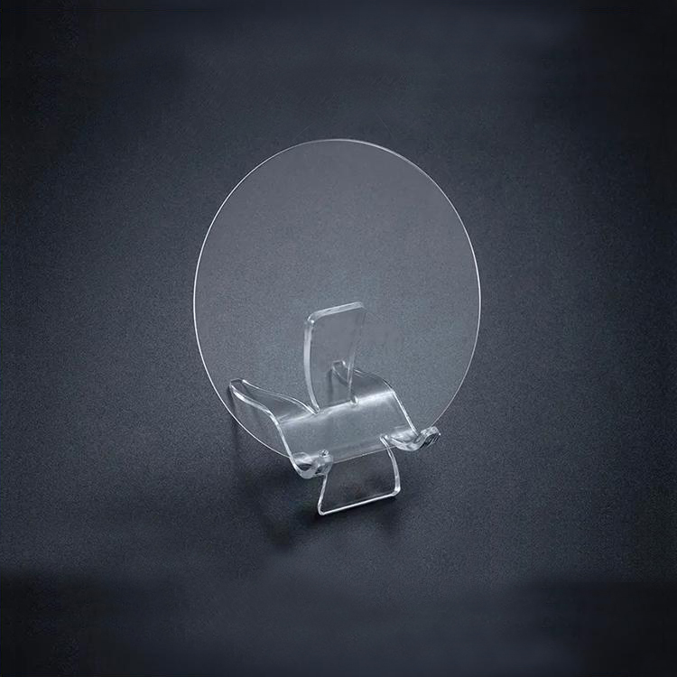
Calcium Fluoride (CaF2) Single Crystal Substrates
- Wide Transmission Range (125 nm–10 μm): Ideal for deep UV, visible, and IR applications.
- Low Refractive Index: Reduces need for anti-reflective coatings.
- Minimal Birefringence: Suitable for precision optical systems.
- High Laser Damage Threshold: Critical for high-power laser optics.
- Excellent Chemical Inertness: Resistant to water, many acids, and most solvents.
- Thermal and Mechanical Stability: Supports use in demanding environments.
- Low Absorption in UV and IR: Maximizes optical throughput.
- Compatibility with Epitaxial Growth: Suitable for specialized semiconductor processes (e.g., GaN on CaF₂ substrates).
- Low Scattering and High Surface Quality: Essential for high-resolution optical systems.
Custom products or bulk orders, please contact us for competitive pricing!
- Satisfaction Guaranteed
- No Hassle Refunds
- Secure Payments
Description
Calcium Fluoride (CaF₂) single crystal substrates are renowned for their exceptional optical transparency across a wide spectral range, from deep ultraviolet (DUV) through infrared (IR). With a low refractive index, minimal birefringence, excellent chemical stability, and high laser damage threshold, CaF₂ crystals are widely used in high-performance optical components, photolithography, laser systems, spectroscopy, and semiconductor manufacturing.
We offer high-quality CaF₂ substrates with customizable sizes, orientations, and surface finishes to meet diverse research and industrial needs.
Crystal Structure and Orientation:
- Chemical Formula: CaF₂
- Crystal System: Cubic (Fluorite structure)
- Lattice Constant: a = 5.462 Å
- Transparency Range: 0.125 µm (125 nm) to 10 µm
- Refractive Index: ~1.4338 at 589 nm
- Density: 3.18 g/cm³
- Hardness (Mohs): 4
- Melting Point: ~1418°C
- Available Orientations:
- (100) Orientation: Standard for epitaxial growth and optical applications
- (111) Orientation: Offers different cleavage and optical properties
- (110) Orientation: Special applications
- Custom orientations available upon request
Key Properties and Advantages:
- Wide Transmission Range (125 nm–10 μm): Ideal for deep UV, visible, and IR applications.
- Low Refractive Index: Reduces need for anti-reflective coatings.
- Minimal Birefringence: Suitable for precision optical systems.
- High Laser Damage Threshold: Critical for high-power laser optics.
- Excellent Chemical Inertness: Resistant to water, many acids, and most solvents.
- Thermal and Mechanical Stability: Supports use in demanding environments.
- Low Absorption in UV and IR: Maximizes optical throughput.
- Compatibility with Epitaxial Growth: Suitable for specialized semiconductor processes (e.g., GaN on CaF₂ substrates).
- Low Scattering and High Surface Quality: Essential for high-resolution optical systems.
Typical Applications:
- Optical windows, lenses, and prisms for UV, visible, and IR systems
- Deep UV lithography (DUV) masks and optics (especially 193 nm wavelength applications)
- Laser optics for high-power laser systems
- Infrared spectroscopy windows and components
- Space-borne optical instruments
- Epitaxial substrate for III-V semiconductor materials
- Vacuum ultraviolet (VUV) optics and instruments
- Beam splitters, polarizers, and filters
- Medical laser systems
- Nonlinear optics and photonics research
Specifications:
| Diameter | 10 mm – 100 mm (larger sizes available) |
| Thickness | 0.2 mm – 5 mm (custom options) |
| Orientation | <100>, <111>, <110>, custom |
| Surface Finish | Optical polish (10-5 or better Scratch-Dig) |
| Surface Flatness | λ/8 or better @ 632.8 nm |
| Parallelism | <10 arc seconds |
| Transmission | >90% from 150 nm to 9 μm |
| Surface Roughness (Ra) | <5 Å (Atomic Force Microscope measurement) |
| Coating Options | AR coating available for UV/IR bands |
| Edge Treatment | Beveled or straight-cut |
Available Sizes and Customization:
- Wafer Sizes: 10 mm, 20 mm, 25 mm, 50 mm, 76.2 mm (3 inch), 100 mm (4 inch), custom
- Thickness Range: 0.2 mm, 0.5 mm, 1 mm, 2 mm, and custom upon request
- Polish Types:
- Single-Side Polished (SSP)
- Double-Side Polished (DSP)
- Orientation Accuracy: ±0.5° standard (higher accuracy available)
- Special Treatments:
- Ultra-flat polishing
- Ultra-clean packaging for semiconductor applications
- Customization: Diameter, thickness, crystal orientation, polishing grade, and coatings can be fully tailored.
Quality Assurance:
Each CaF₂ substrate undergoes comprehensive inspection and quality control, including:
- X-ray Diffraction (XRD) for crystal orientation verification
- Spectrophotometry for transmission evaluation
- Interferometry for surface flatness measurement
- Surface inspection for scratches, digs, and defects under high magnification
- Thickness and parallelism verification
- Cleanroom (Class 100) packaging to ensure contamination-free delivery
Why Choose Our Calcium Fluoride (CaF₂) Substrates?
- Superior crystal growth technology ensuring low defect density
- Wide transparency range with ultra-high optical quality
- Custom manufacturing according to your specifications
- Rapid delivery and competitive pricing for research and production scale
- Strong technical support and guidance for your application needs
- Proven reliability across industries such as optics, semiconductors, aerospace, and defense
Ordering & Contact Information:
We offer flexible MOQ (Minimum Order Quantity) and competitive pricing. Our substrates are packaged in Class 100 cleanroom environments and shipped worldwide. For custom orders or technical inquiries, please contact us for a detailed consultation!
Related products
-

-

-

-
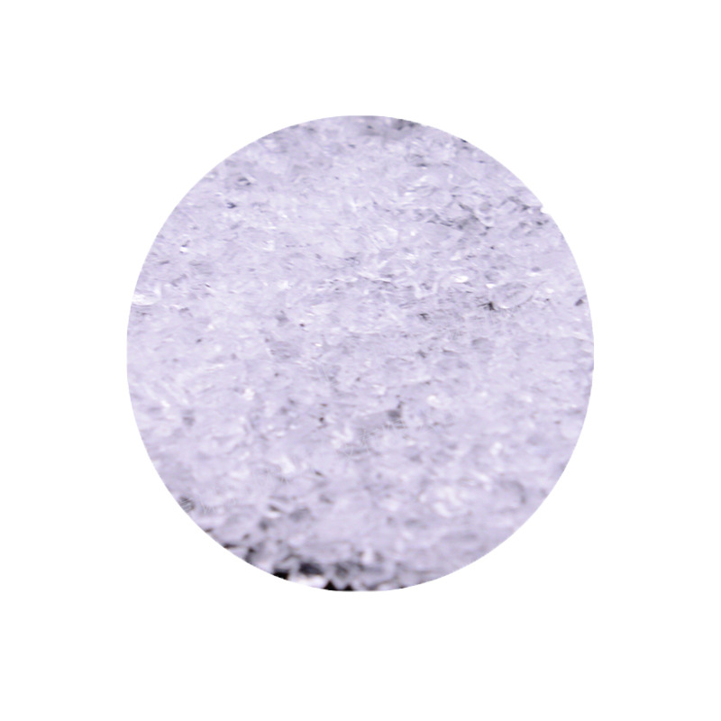
Cryolite (Na3AlF6, Sodium Aluminum Fluoride) Granules / Pellets 99.99% – Size 1–3 mm | Custom Purity & Particle Size Available
$105.00 – $495.00Select options This product has multiple variants. The options may be chosen on the product page