Single Crystal Substrates - Tinsan Materials")


 Single Crystal - Tinsan Materials")
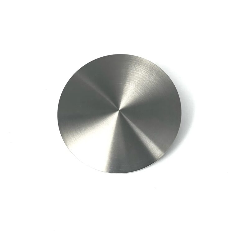
Copper (Cu) Single Crystal Substrates
- High Electrical Conductivity: One of the highest among metals (~5.96×10⁷ S/m at 20°C)
- Excellent Thermal Conductivity: ~400 W/m·K
- Surface Smoothness: Atomically flat surfaces achievable after polishing
- Superior Purity Levels: Available in 99.999% (5N) or higher grades
- Stable Crystallographic Surface: Ideal for reproducible surface-sensitive experiments
- Low Surface Roughness: Ra < 5 Å achievable for polished samples
- Strong Corrosion Resistance: Protective native oxide layer forms naturally under ambient conditions
- Easily Customizable: Wide range of sizes, thicknesses, and orientations available
Custom products or bulk orders, please contact us for competitive pricing!
- Satisfaction Guaranteed
- No Hassle Refunds
- Secure Payments
Description
Copper (Cu) single crystals are high-purity materials characterized by a continuous, defect-free atomic structure throughout the entire specimen. Featuring a face-centered cubic (FCC) lattice and exceptional thermal and electrical conductivity, Copper single crystals serve as ideal substrates for surface science research, thin film epitaxy, graphene growth, catalysis studies, and material physics. Their well-defined crystallographic surfaces provide a highly controllable and reproducible platform for advanced research applications requiring atomic-level precision.
Crystal Structure and Orientation:
- Crystal System: Face-Centered Cubic (FCC)
- Space Group: Fm-3m (No. 225)
- Lattice Constant: a = 3.615 Å
- Density: 8.96 g/cm³
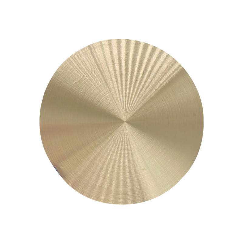
- Surface Orientations Available:
- (100)
- (110)
- (111)
- Custom orientations (e.g., (210), (311)) upon request
Each substrate is cut precisely with an orientation accuracy of ±0.5° or better to ensure optimal performance in demanding research environments.
Key Properties and Advantages:
- High Electrical Conductivity: One of the highest among metals (~5.96×10⁷ S/m at 20°C)
- Excellent Thermal Conductivity: ~400 W/m·K
- Surface Smoothness: Atomically flat surfaces achievable after polishing
- Superior Purity Levels: Available in 99.999% (5N) or higher grades
- Stable Crystallographic Surface: Ideal for reproducible surface-sensitive experiments
- Low Surface Roughness: Ra < 5 Å achievable for polished samples
- Strong Corrosion Resistance: Protective native oxide layer forms naturally under ambient conditions
- Easily Customizable: Wide range of sizes, thicknesses, and orientations available
Typical Applications:
- Graphene growth via chemical vapor deposition (CVD)
- Thin film epitaxy of metals, oxides, and 2D materials
- Surface physics and chemistry studies
- Catalysis research (e.g., CO₂ reduction, hydrogen evolution)
- Electron microscopy calibration and diffraction experiments
- Ultra-High Vacuum (UHV) surface science
- Quantum materials research
- Electrical and thermal property investigations at the nanoscale
Specifications:
| Purity | ≥99.999% (5N), optional higher grades |
| Orientation Accuracy | ±0.5° (higher precision available) |
| Thickness Tolerance | ±0.05 mm |
| Surface Finish | Polished (Ra < 5 Å) or As-cut |
| Available Sizes | 5mm × 5mm, 10mm × 10mm, Ø10mm-Ø50mm, Custom sizes |
| Surface Orientations | (100), (110), (111), Custom |
| Packaging | Class 100 cleanroom vacuum packaging |
Optional treatments include surface cleaning (e.g., electrochemical polishing), annealing, and oxide layer removal under UHV conditions.
Available Sizes and Customization:
We offer standard and customized Copper single crystals:
- Rectangular or square substrates
- Round wafers up to Ø50mm
- Thickness ranging from 0.3mm to several millimeters
- Special request: ultra-thin foils for flexible substrate applications
Custom specifications such as miscut angles, double-side polishing, special crystallographic orientations, and oxide-free surfaces are available upon request to meet specialized research needs.
Quality Assurance:
Every Copper single crystal substrate undergoes rigorous quality control, including:
- High-resolution X-ray Diffraction (HRXRD) for orientation verification
- Electron Backscatter Diffraction (EBSD) (optional) for surface mapping
- Atomic Force Microscopy (AFM) for surface roughness analysis
- Visual inspection under cleanroom conditions
- Purity certification and detailed inspection reports
All products are processed and packaged under ISO Class 100 cleanroom conditions to ensure minimal contamination and oxidation.
Why Choose Our Copper Single Crystals?
- High-purity copper ensures excellent electrical and thermal properties
- Ultra-smooth, precisely oriented surfaces ideal for critical research
- Comprehensive size and orientation customization available
- Fast delivery times and competitive pricing
- Full technical support for substrate handling, surface preparation, and UHV applications
Ordering & Contact Information:
We offer flexible MOQ (Minimum Order Quantity) and competitive pricing. Our substrates are packaged in Class 100 cleanroom environments and shipped worldwide. For custom orders or technical inquiries, please contact us for a detailed consultation!