Single Crystal Substrate - Tinsan Materials")

 Single Crystal - Tinsan Materials")
LSAT Single Crystal Substrates
- Excellent Lattice Matching: Ideal match for many perovskite oxides such as YBCO, BST, and PZT
- High Thermal Stability: Maintains structural integrity under high temperatures
- Low Dielectric Loss: Suitable for microwave and dielectric applications
- High Crystallinity: Enables defect-free epitaxial film growth
- Good Mechanical Strength: Durable for various thin-film deposition processes
- Smooth Surface Finish: Atomic-level flatness for epitaxial growth
- High Chemical Stability: Resists degradation during processing
- Wide Application Range: Compatible with superconducting, ferroelectric, and oxide-based systems
Custom products or bulk orders, please contact us for competitive pricing!
- Satisfaction Guaranteed
- No Hassle Refunds
- Secure Payments
Description
Lanthanum Strontium Aluminum Tantalate (LSAT) single crystal substrates are high-quality oxide materials primarily used for the epitaxial growth of high-temperature superconducting films, ferroelectric films, and oxide-based thin films. LSAT substrates exhibit excellent lattice matching with many perovskite-structured materials, possess high thermal stability, low dielectric losses, and maintain high crystallinity even under demanding processing conditions. Their superior surface quality and stability make them ideal for advanced research and industrial production in fields like superconductivity, magneto-optics, and microelectronics.
Crystal Structure and Orientation:
- Crystal System: Perovskite-type structure, pseudocubic
- Space Group: Pm-3m
- Lattice Parameter (Pseudocubic): a ≈ 3.756 Å
- Thermal Expansion Coefficient: ~9×10⁻⁶/K
- Available Surface Orientations:
- (100)
- (110)
- (111)
- Custom orientations and miscut angles available upon request.
Key Properties and Advantages:
- Excellent Lattice Matching: Ideal match for many perovskite oxides such as YBCO, BST, and PZT
- High Thermal Stability: Maintains structural integrity under high temperatures
- Low Dielectric Loss: Suitable for microwave and dielectric applications
- High Crystallinity: Enables defect-free epitaxial film growth
- Good Mechanical Strength: Durable for various thin-film deposition processes
- Smooth Surface Finish: Atomic-level flatness for epitaxial growth
- High Chemical Stability: Resists degradation during processing
- Wide Application Range: Compatible with superconducting, ferroelectric, and oxide-based systems
Typical Applications:
- High-temperature superconducting thin film growth (e.g., YBCO, Bi-2212)
- Epitaxial growth of ferroelectric and piezoelectric films (e.g., PZT, BST)
- Oxide electronic devices
- Dielectric resonators and microwave devices
- Optical and electro-optical device research
- Thin film capacitors and memory devices
- Fundamental studies of complex oxide materials
- Multilayer heterostructure device development
Specifications:
| Purity | ≥99.99% (4N) |
| Orientation Accuracy | ±0.5° (higher precision available) |
| Thickness Tolerance | ±0.02 mm |
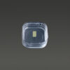
| Surface Finish | Single-side polished (SSP) or double-side polished (DSP) |
| Surface Roughness (Ra) | <0.5 nm (AFM measurement) |
| Size Range | 10×10mm, 15×15mm, 20×20mm, Ø1″, Ø2″ (custom sizes available) |
| Surface Orientations | (100), (110), (111), custom |
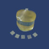
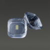
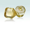
| Packaging | Class 100 cleanroom vacuum sealed |
Available Sizes and Customization:
- Square substrates: 10×10mm, 15×15mm, 20×20mm, 5×5mm available for research samples
- Round wafers: Ø25.4mm (1 inch), Ø50.8mm (2 inch)
- Thickness options: 0.3mm, 0.5mm, 1.0mm (other thicknesses on request)
- Surface Options: Single-side polished (SSP) or Double-side polished (DSP)
- Customization:
- Special crystallographic orientations and miscut angles
- Ultra-thin or thicker customized substrates
- Thermal treatment (annealing) to reduce dislocations
- Laser marking or edge treatment (chamfered or beveled edges)
We support R&D and mass production customization for both academic and industrial applications.
Quality Assurance:
Each LSAT substrate is subjected to strict quality control procedures:
- Orientation verified by high-resolution X-ray diffraction (HRXRD)
- Surface quality tested by atomic force microscopy (AFM)
- Purity analysis using glow discharge mass spectrometry (GDMS)
- Optical microscopy inspection to ensure no scratches, chips, or inclusions
- Dimensional verification with precision metrology
- Thickness and flatness tests to meet exact specifications
- Vacuum packing in a Class 100 cleanroom environment
A full Certificate of Compliance (CoC) is provided with every delivery to ensure traceability.
Why Choose Our LSAT Single Crystal Substrates?
- Outstanding lattice match with perovskite oxide materials
- Superior surface quality for high-quality epitaxial growth
- Flexible sizing and customization options
- Reliable and fast lead times for research and production orders
- Professional technical support and after-sales service
- Competitive pricing without compromising quality
Ordering & Contact Information:
We offer flexible MOQ (Minimum Order Quantity) and competitive pricing. Our substrates are packaged in Class 100 cleanroom environments and shipped worldwide. For custom orders or technical inquiries, please contact us for a detailed consultation!