Single Crystal Substrates - Tinsan Materials")


LiAlO2 (Lithium Aluminate) Single Crystal Substrates
- High Thermal Stability: Excellent performance under high temperatures up to 1500°C.
- Wide Bandgap: Enables use in deep UV and high-power electronic applications.
- Superior Mechanical Strength: Resists thermal shock and mechanical stress.
- Excellent Lattice Match: Ideal substrate for GaN, AlN, ZnO, and other oxide semiconductor epitaxial growth.
- Low Dielectric Loss: Beneficial for microwave and RF device applications.
- Chemical Inertness: High resistance to acids, alkalis, and environmental degradation.
- Smooth, Defect-Free Surface: Essential for high-yield epitaxial growth and thin-film deposition.
Custom products or bulk orders, please contact us for competitive pricing!
- Satisfaction Guaranteed
- No Hassle Refunds
- Secure Payments
Description
Lithium Aluminate (LiAlO₂) is a high-quality single crystal material with outstanding thermal stability, mechanical strength, and excellent lattice matching properties.
Due to its unique combination of physical and chemical characteristics, LiAlO₂ single crystal substrates are widely utilized in the fields of epitaxial growth, optoelectronics, semiconductor devices, and advanced materials research.
We supply top-grade LiAlO₂ substrates with precisely controlled crystallographic orientation, ultra-smooth surfaces, and minimal defect densities to meet the requirements of high-performance applications.
Crystal Structure and Orientation:
- Chemical Formula: LiAlO₂
- Crystal Structure: Tetragonal (α-LiAlO₂) or Rhombohedral (γ-LiAlO₂)
- Space Group:
- α-LiAlO₂: I41/amd
- γ-LiAlO₂: R-3m
- Lattice Constants:
- α-LiAlO₂: a = 5.169 Å, c = 6.267 Å
- γ-LiAlO₂: a = 2.808 Å, c = 14.209 Å
- Density: ~2.62 g/cm³
- Melting Point: ~1620°C
- Bandgap: ~6.2 eV (wide bandgap)
- Available Orientations:
- (001), (100), (110), (111) — tailored to different epitaxial requirements
Key Properties and Advantages:
- High Thermal Stability: Excellent performance under high temperatures up to 1500°C.
- Wide Bandgap: Enables use in deep UV and high-power electronic applications.
- Superior Mechanical Strength: Resists thermal shock and mechanical stress.
- Excellent Lattice Match: Ideal substrate for GaN, AlN, ZnO, and other oxide semiconductor epitaxial growth.
- Low Dielectric Loss: Beneficial for microwave and RF device applications.
- Chemical Inertness: High resistance to acids, alkalis, and environmental degradation.
- Smooth, Defect-Free Surface: Essential for high-yield epitaxial growth and thin-film deposition.
Typical Applications:
- Epitaxial growth of wide-bandgap semiconductors (e.g., GaN, AlN, ZnO thin films)
- Substrate for deep ultraviolet (DUV) optoelectronic devices
- High-temperature and high-frequency electronics
- Transparent conductive oxide (TCO) film deposition
- Photonic and laser devices
- Research on ferroelectric and piezoelectric thin films
- Microwave and radio-frequency (RF) device components
- Substrate for neutron detectors and radiation-resistant devices
Specifications:
| Material | Lithium Aluminate (LiAlO₂) |
| Crystal Structure | Tetragonal (α-LiAlO₂) or Rhombohedral (γ-LiAlO₂) |
| Orientation | (001), (100), (110), (111) |
| Lattice Constants (α-phase) | a = 5.169 Å, c = 6.267 Å |
| Density | ~2.62 g/cm³ |
| Melting Point | ~1620°C |
| Bandgap | ~6.2 eV |
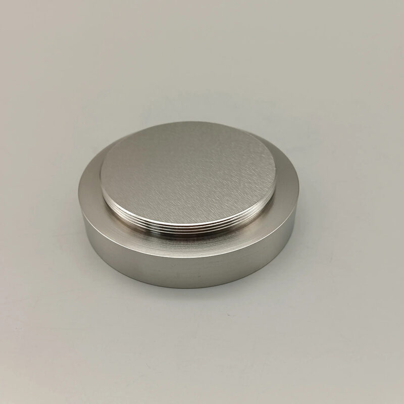
| Standard Sizes | 10×10 mm², 20×20 mm², 1 inch, 2 inches |
| Thickness | 0.5 mm, 1 mm, 2 mm (customizable) |
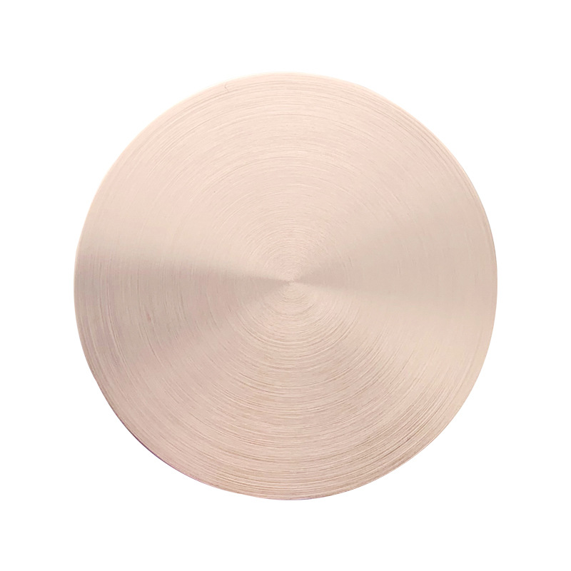
| Surface Finish | Double-Side Polished (DSP) |
| Surface Quality | 10-5 or 20-10 Scratch-Dig (MIL-PRF-13830B) |
| Surface Flatness | λ/10 @ 632.8 nm |
| Parallelism | < 10 arc seconds |
| Orientation Accuracy | ±0.5° |
| Defect Density | Very Low (Epi-Ready Quality) |
| Available Surface Treatment | DSP standard, SSP on request |
| Application Areas | Epitaxial growth, optoelectronics, semiconductors, DUV devices, microwave devices |
| Customization | Size, orientation, thickness, and surface finish customizable |
Available Sizes and Customization:
- Standard Substrate Sizes:
- 10 × 10 mm²
- 15 × 15 mm²
- 20 × 20 mm²
- 1 inch, 2 inches diameter
- Custom Sizes:
- Special shapes (e.g., squares, rectangles, circles) and thicknesses can be customized according to project needs.
- Thickness Options:
- 0.3 mm, 0.5 mm, 1.0 mm, 2.0 mm standard, others upon request
- Surface Options:
- Double-Side Polished (DSP) standard
- Single-Side Polished (SSP) available upon special request
- Edge Options:
- Laser cut, beveled, or rounded edges for mechanical safety
Quality Assurance:
We employ rigorous quality control processes to ensure the best performance of our LiAlO₂ substrates:
- High-Resolution X-Ray Diffraction (HRXRD) to verify crystal orientation and purity
- Atomic Force Microscopy (AFM) to ensure nanometer-level surface smoothness
- Optical Microscopy and Surface Inspection to eliminate defects and contamination
- Cleanroom Class 1000 packaging to avoid particle contamination
Why Choose Our LiAlO₂ Single Crystal Substrates?
- Premium crystalline quality with ultra-low defect densities
- Excellent thermal, mechanical, and chemical stability
- Epi-ready polishing for high-quality thin film growth
- Flexible size, orientation, and thickness customization
- Short lead time and competitive pricing
- Full technical support and responsive customer service
Ordering & Contact Information:
Tinsan Materials offers flexible MOQ (Minimum Order Quantity) and competitive pricing. Our substrates are packaged in Class 100 cleanroom environments and shipped worldwide. For custom orders or technical inquiries, please contact us for a detailed consultation!