Lithium Niobate (LiNbO3) Wafers
- High Electro-optic Coefficient: Enables efficient light modulation
- Excellent Nonlinear Optical Properties: Ideal for frequency conversion processes
- Wide Transmission Range: Suitable for UV, visible, and infrared applications
- Strong Piezoelectric Response: Essential for SAW and MEMS devices
- Photorefractive Effect: Useful for holography and optical data storage
- Chemical and Thermal Stability: High reliability in demanding environments
- Availability of Stoichiometric and MgO-doped Variants: Reduces photorefractive damage and enhances performance in high-power lasers
- Precise Crystal Growth and Wafer Fabrication: Ensures high uniformity and low defect densities
Custom products or bulk orders, please contact us for competitive pricing!
- Satisfaction Guaranteed
- No Hassle Refunds
- Secure Payments
Description
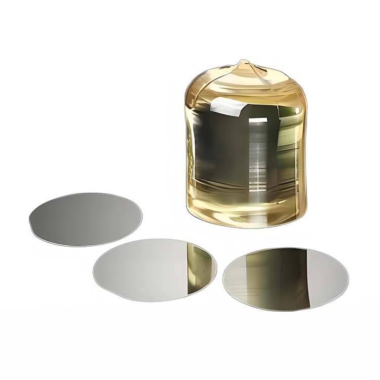
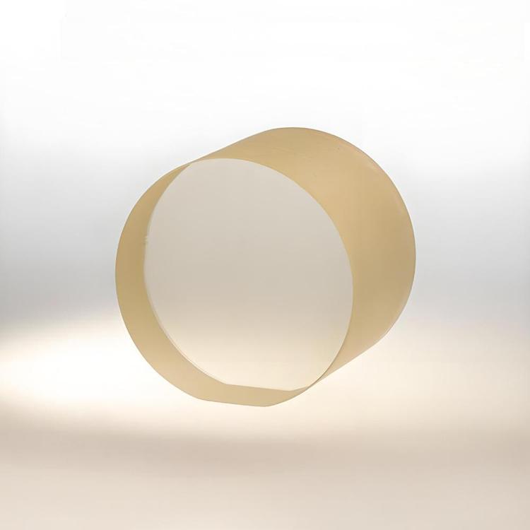
Lithium Niobate (LiNbO₃) is a ferroelectric crystal material well-known for its excellent electro-optic, nonlinear optical, piezoelectric, and photorefractive properties. As a key substrate for integrated optics and nonlinear optical devices, Lithium Niobate wafers are widely used in optical modulators, frequency doublers, surface acoustic wave (SAW) devices, and emerging photonic integrated circuits (PICs).
Available in congruent, near-stoichiometric, and stoichiometric compositions, Lithium Niobate wafers support applications in the telecommunications, laser, quantum optics, and sensing industries.
Crystal Structure and Orientation:
- Chemical Formula: LiNbO₃
- Crystal System: Trigonal (Space group R3c)
- Transparency Range: 330 nm – 5200 nm
- Refractive Indices:
- no = 2.286 (at 1064 nm)
- ne = 2.203 (at 1064 nm)
- Electro-optic Coefficients:
- r₃₃ ≈ 30.8 pm/V
- Curie Temperature: ~1140 °C
- Density: 4.64 g/cm³
- Hardness (Mohs): ~5
- Melting Point: ~1255 °C
- Available Orientations:
- Z-cut (most common, for electro-optic modulation and nonlinear optics)
- X-cut (used in piezoelectric and acoustic wave devices)
- Y-cut and custom orientations available upon request
Key Properties and Advantages:
- High Electro-optic Coefficient: Enables efficient light modulation
- Excellent Nonlinear Optical Properties: Ideal for frequency conversion processes
- Wide Transmission Range: Suitable for UV, visible, and infrared applications
- Strong Piezoelectric Response: Essential for SAW and MEMS devices
- Photorefractive Effect: Useful for holography and optical data storage
- Chemical and Thermal Stability: High reliability in demanding environments
- Availability of Stoichiometric and MgO-doped Variants: Reduces photorefractive damage and enhances performance in high-power lasers
- Precise Crystal Growth and Wafer Fabrication: Ensures high uniformity and low defect densities
Typical Applications:
- Electro-optic modulators (EOMs) for fiber optic communication
- Second harmonic generation (SHG) and optical parametric oscillators (OPO)
- Surface acoustic wave (SAW) and bulk acoustic wave (BAW) devices
- Photonic integrated circuits (PICs)
- Quantum optics and single-photon sources
- Terahertz generation and detection
- Holographic storage and optical signal processing
- Sensors and micro-electro-mechanical systems (MEMS)
Specifications:
| Crystal Type | Congruent, Stoichiometric, MgO-doped |
| Orientation | Z-cut, X-cut, Y-cut, custom cuts |
| Diameter | 2″, 3″, 4″, 6″ (other sizes available) |
| Thickness | 0.2 mm to 1 mm (customizable) |
| Surface Roughness | <1 nm RMS (for optical grade polishing) |
| Surface Quality | 10-5 scratch/dig (MIL-PRF-13830B) |
| Flatness | λ/8 or better @ 632.8 nm |
| Parallelism | <20 arc seconds |
| Bow/Warp | <10 μm (depending on size and thickness) |
| Coatings | AR coatings for telecom bands, SHG wavelengths available |
| Dopant Options | MgO (typically 5 mol% or customizable) |
Available Sizes and Customization:
- Diameters: 2-inch, 3-inch, 4-inch, and 6-inch wafers, custom
- Standard Thicknesses: 500 μm, 1000 μm (custom thicknesses from 200 μm–>2 mm available)
- Polish Options:
- Single-side polished (SSP)
- Double-side polished (DSP)
- Orientation Precision: ±0.5° standard (higher precision available)
- AR Coatings: Available for telecom bands (1310 nm, 1550 nm) and SHG wavelengths
- Doping: MgO-doping (typically 5 mol%) available for improved damage resistance
- Custom Cutting and Dicing: Available upon request
Quality Assurance:
All our Lithium Niobate wafers undergo strict quality control to ensure optimal performance:
- X-ray diffraction (XRD) for orientation and crystallinity verification
- Surface flatness measured by interferometry
- Surface quality inspection under high-magnification optical microscopes
- Coating adhesion and durability tested to international standards
- Thickness, roughness, and uniformity measurements reported
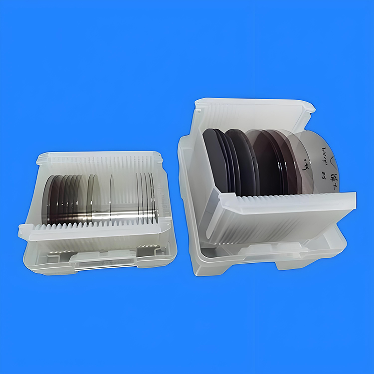
- Packaged in cleanroom environments (Class 100) to prevent contamination
Why Choose Our Lithium Niobate Wafers?
- High-quality crystal growth with low defect density
- Precision cutting, polishing, and surface finishing
- Availability of congruent, stoichiometric, and MgO-doped options
- Flexible customization to meet specific project requirements
- Competitive pricing and fast lead times
- Technical support for integration into optical, electronic, and photonic systems
Ordering & Contact Information:
We offer flexible MOQ (Minimum Order Quantity) and competitive pricing. Our wafers are packaged in Class 100 cleanroom environments and shipped worldwide. For custom orders or technical inquiries, please contact us for a detailed consultation!
