Single Crystal Substrate - Tinsan Materials")
 Single Crystal Substrates - Tinsan Materials")

Magnesium Oxide (MgO) Single Crystal Substrates
- Excellent lattice matching for oxide thin films
- Wide transparency from UV to IR regions (0.3μm–6μm)
- High thermal conductivity and melting point (2852°C)
- Chemically inert to most acids and alkalis
- Low dielectric constant (ε ≈ 9.65 at 1MHz)
Custom products or bulk orders, please contact us for competitive pricing!
- Satisfaction Guaranteed
- No Hassle Refunds
- Secure Payments
Description
Magnesium Oxide (MgO) substrates are high-quality single-crystal materials renowned for their excellent lattice matching, superior thermal conductivity, chemical stability, and optical transparency across a wide spectral range.
MgO substrates are ideal for epitaxial growth of high-temperature superconductors (HTS), ferroelectric thin films, and various oxide-based electronic devices. Thanks to their low dielectric constant and high melting point, MgO substrates are also highly suited for RF and microwave device applications.
Key Characteristics:
- Excellent lattice matching for oxide thin films
- Wide transparency from UV to IR regions (0.3μm–6μm)
- High thermal conductivity and melting point (2852°C)
- Chemically inert to most acids and alkalis
- Low dielectric constant (ε ≈ 9.65 at 1MHz)
Specifications & Properties:
| Material | Single Crystal Magnesium Oxide (MgO) |
| Crystal Structure | Cubic (Rock Salt Structure, Fm-3m) |
| Crystal Orientation | <100>, <110>, <111> |
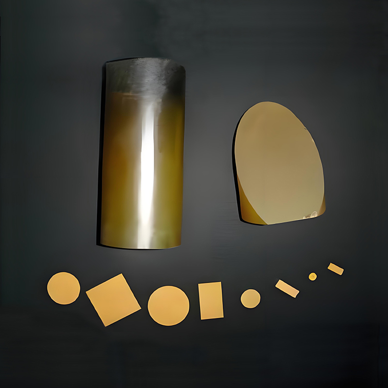
| Diameter/Size | 10mm × 10mm, 20mm × 20mm, 2″, 3″, 4″ (custom sizes available) |
| Thickness | 0.5mm, 1mm, 2mm (other thicknesses upon request) |
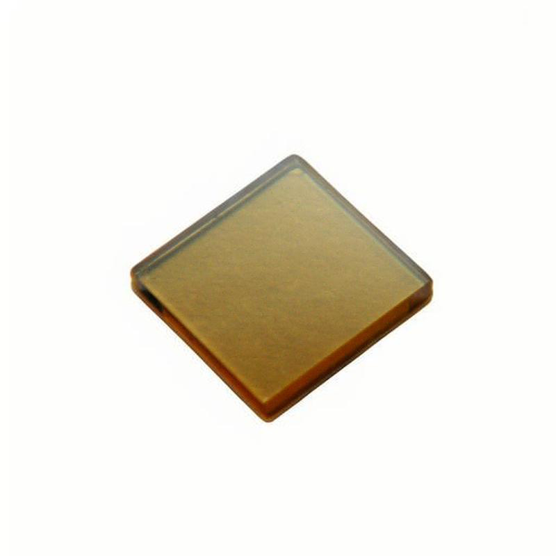
| Surface Finish | Single-side polished (SSP), Double-side polished (DSP), As-cut |
| Surface Roughness | < 5Å (Atomic level, on polished surfaces) |
| Orientation Tolerance | ±0.5° or customized |
| Flatness | < 5µm (for 2-inch wafer, custom available) |
| BOW/TTV | According to SEMI standard or customized |
| Transmission Range | 0.3µm – 6.0µm |
All wafers comply with international standards and can be customized for specialized research and industrial applications.
Crystal Orientations & Applications:
① <100> Orientation
- Properties: Symmetric surface, commonly used for epitaxial growth.
- Applications: High-Tc superconducting thin films (YBCO, BSCCO), ferroelectric and oxide electronics.
② <110> Orientation
- Properties: Anisotropic lattice suitable for specific heteroepitaxy applications.
- Applications: Complex oxide thin films, novel heterostructures.
③ <111> Orientation
- Properties: Close-packed structure ideal for certain epitaxial layer developments.
- Applications: Advanced research in quantum devices, optoelectronic materials.
Key Advantages:
- Superior Thermal Stability – Usable up to extremely high temperatures (~2000°C operational stability).
- Excellent Optical Transparency – Transmits from UV to mid-infrared wavelengths.
- Good Lattice Match – Suitable for perovskite oxides, superconducting, and ferroelectric materials.
- Low Dielectric Loss – Essential for RF, microwave, and communication device fabrication.
- Chemically Resistant – High resistance to acid and alkali corrosion.
- High-Quality Surfaces – Ultra-smooth polished surfaces ideal for epitaxial film deposition.
Applications:
- High-Temperature Superconductors (HTS) – YBa₂Cu₃O₇₋ₓ (YBCO) thin films.
- Ferroelectric Films – BST (Barium Strontium Titanate), PZT (Lead Zirconate Titanate) devices.
- Oxide Electronics – Epitaxial complex oxides for novel devices.
- Spintronics & Quantum Research – MgO tunneling barriers in MTJs (magnetic tunnel junctions).
- Optical Windows – For high-power laser and infrared applications.
- Microwave and RF Devices – Filters, resonators, substrates for high-frequency circuits.
Customization Options:
We offer fully tailored MgO substrates to meet unique application needs:
- Size: 10×10mm, 20×20mm, 2″, 3″, 4″ wafers, or custom sizes.
- Orientation: <100>, <110>, <111> – other custom cuts available.
- Thickness: 0.5mm to 2mm standard, others upon request.
- Polishing: SSP (Single Side Polished), DSP (Double Side Polished).
- Surface Quality:
- Atomic-scale roughness (<5Å Ra available).
- High flatness for demanding film growth.
- Edge Options: Ground, beveled, or chamfered.
- Special Coatings: Optional surface treatments like anti-reflective (AR) coatings.
Volume manufacturing and small-batch R&D orders are both available with short lead times.
Quality & Certifications:
Every substrate undergoes strict quality control to ensure top-notch performance:
- ISO 9001 Certified production processes.
- SEMI Standards for flatness, thickness uniformity, orientation precision.
- Complete Quality Inspection: Including surface roughness, XRD analysis for crystal quality, and laser flatness measurement.
- RoHS and REACH Compliant: Eco-friendly manufacturing.
- Cleanroom Packaging: Class 100 packaging ensures wafer cleanliness.
Detailed inspection reports are available with each order to guarantee traceability and reliability.
Ordering & Contact Information:
We offer flexible MOQ (Minimum Order Quantity) and competitive pricing. Our substrates are packaged in Class 100 cleanroom environments and shipped worldwide. For custom orders or technical inquiries, please contact us for a detailed consultation!