Wafers - Tinsan Materials")


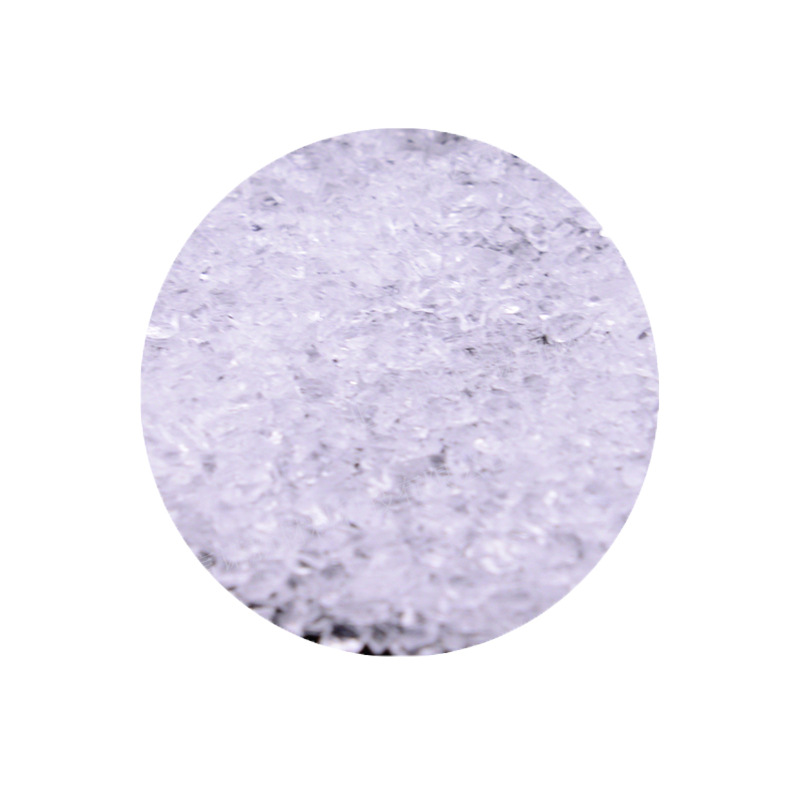
Sapphire (Al2O3) Wafers
- Extreme surface hardness (Mohs 9, second only to diamond)
- Wide optical transmission from 150 nm (UV) to 5.5 μm (MWIR)
- High thermal conductivity and thermal shock resistance
- Excellent chemical inertness against acids and alkalis
- High dielectric strength and electrical insulation properties
Custom products or bulk orders, please contact us for competitive pricing!
- Satisfaction Guaranteed
- No Hassle Refunds
- Secure Payments
Description
Sapphire wafers are single-crystal aluminum oxide (Al₂O₃) substrates known for their exceptional hardness, chemical resistance, high-temperature stability, and wide optical transmission range. They are widely used in semiconductor, LED, RFIC, optical, and sensor applications.
Our sapphire wafers are available in a variety of sizes, orientations, thicknesses, and surface finishes to meet the rigorous requirements of different industries.
Key Characteristics:
-
Extreme surface hardness (Mohs 9, second only to diamond)
-
Wide optical transmission from 150 nm (UV) to 5.5 μm (MWIR)
-
High thermal conductivity and thermal shock resistance
-
Excellent chemical inertness against acids and alkalis
-
High dielectric strength and electrical insulation properties
Specifications & Properties:
| Material | Single Crystal Sapphire (Al₂O₃) |
| Crystal Structure | Hexagonal (Rhombohedral) |
| Crystal Orientation | C-plane (0001), A-plane (11-20), R-plane (1-102), M-plane (10-10), Custom |
| Diameter | 2″ (50.8mm), 3″, 4″, 6″, 8″, up to 12″ (300mm) |
| Thickness | 100µm – 1500µm (Customizable) |
| Surface Finish | Single-side polished (SSP), Double-side polished (DSP), As-cut |
| Surface Roughness | < 0.5nm Ra (Polished) |
| Flatness | < 5µm (typical, depends on wafer size) |
| BOW/TTV | SEMI standards or customized |
| Orientation Tolerance | ±0.5° or customized |
| Edge Treatment | Rounded or beveled edges |
| Transmission Range | 150nm – 5500nm (UV to IR) |
All wafers are manufactured to comply with SEMI standards unless otherwise specified.
Crystal Orientations & Applications:
① C-plane (0001)
- Properties: Highest symmetry, natural cleavage plane, widely used.
- Applications: LED epitaxy, RFIC substrates, optical windows, semiconductor devices.
② A-plane (11-20)
- Properties: Anisotropic properties ideal for certain epitaxial layers.
- Applications: GaN-based devices, optical substrates requiring specific thermal expansion properties.
③ R-plane (1-102)
- Properties: Suitable for hetero-epitaxial growth of silicon films.
- Applications: Silicon-on-sapphire (SOS) CMOS circuits, specialized optoelectronics.
④ M-plane (10-10)
- Properties: Non-polar plane, used for advanced optical applications.
- Applications: Non-polar GaN epitaxy, advanced photonic devices.
Key Advantages:
- Outstanding Hardness – Resistance to scratching and mechanical wear.
- Wide Transparency Range – UV, visible, and infrared applications.
- High Thermal Stability – Suitable for high-temperature processes (>2000°C melting point).
- Excellent Chemical Resistance – Withstands acids, alkalis, and harsh environments.
- Electrical Insulation – Ideal for microelectronic and RF applications.
- Superior Surface Quality – Ultra-flat polishing available for precision applications.
Applications:
- LED Industry – Sapphire substrates for GaN-based blue, green, and UV LEDs.
- Semiconductors – Substrates for Silicon-on-Sapphire (SOS) ICs, RFICs.
- Optics – Windows and lenses for UV, visible, and IR optics.
- Wearables & Smart Devices – Sapphire covers and sensors for durability.
- Medical Technology – Optical windows for laser and diagnostic equipment.
- Scientific Research – Advanced optics, spectroscopy, and cryogenic applications.
Customization Options:
We provide custom-engineered sapphire wafers to match the unique requirements of your projects:
- Diameter: 2″, 3″, 4″, 6″, 8″, 12″ (or custom).
- Orientation: C-plane, A-plane, R-plane, M-plane, custom angles.
- Thickness: Ultra-thin to ultra-thick wafers (100μm to 1500μm).
- Polishing: Single-side or double-side; ultra-flat options available.
- Surface Quality:
- High precision flatness, minimal TTV/BOW/WARP.
- Low surface roughness (<0.5nm Ra for optical grade).
✔ Edge Profile: Ground, beveled, or laser-cut edges.
✔ Coatings: Anti-reflective (AR) coatings, custom dielectric coatings available upon request.
We are capable of volume production as well as small batch prototyping based on your needs.
Quality & Certifications:
Our sapphire wafers meet the highest international standards:
- ISO 9001 Certified – Robust quality management system.
- SEMI Standard Compliant – Global wafer specification standards.
- RoHS & REACH Compliant – Environmentally responsible production.
- Class 100 Cleanroom Processing – Ultra-clean production and packaging environment.
- Full Inspection Reports – Thickness, flatness, roughness, orientation accuracy, resistivity (if applicable).
Each batch is subjected to stringent quality control to ensure defect-free, high-performance wafers.
Ordering & Contact Information:
We offer flexible MOQ (Minimum Order Quantity) and competitive pricing. Our wafers are packaged in Class 100 cleanroom environments and shipped worldwide. For custom orders or technical inquiries, please contact us for a detailed consultation!
Related products
-
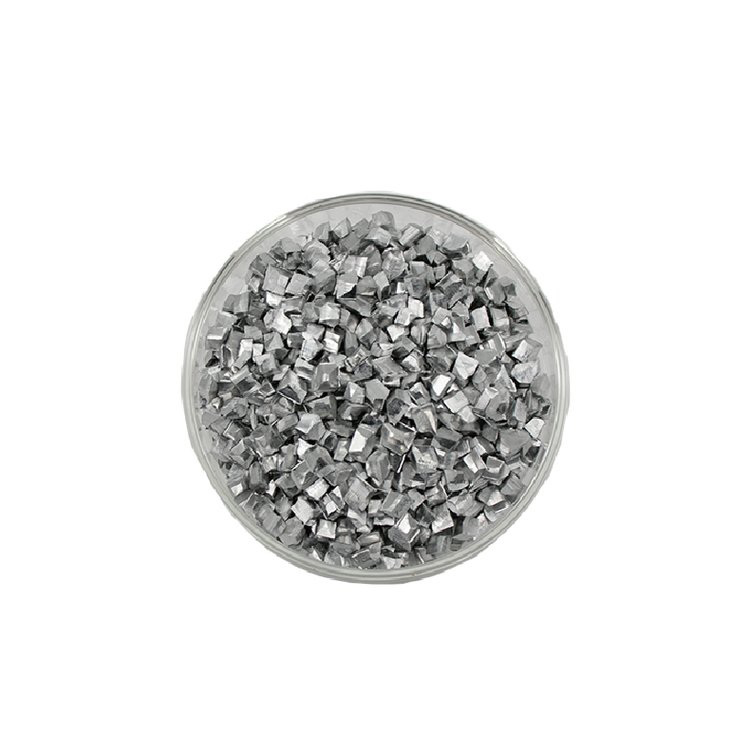

AlSi (Aluminum Silicon) Pellets Granules Evaporation Materials
$1.00 – $375.00Select options This product has multiple variants. The options may be chosen on the product page -

-
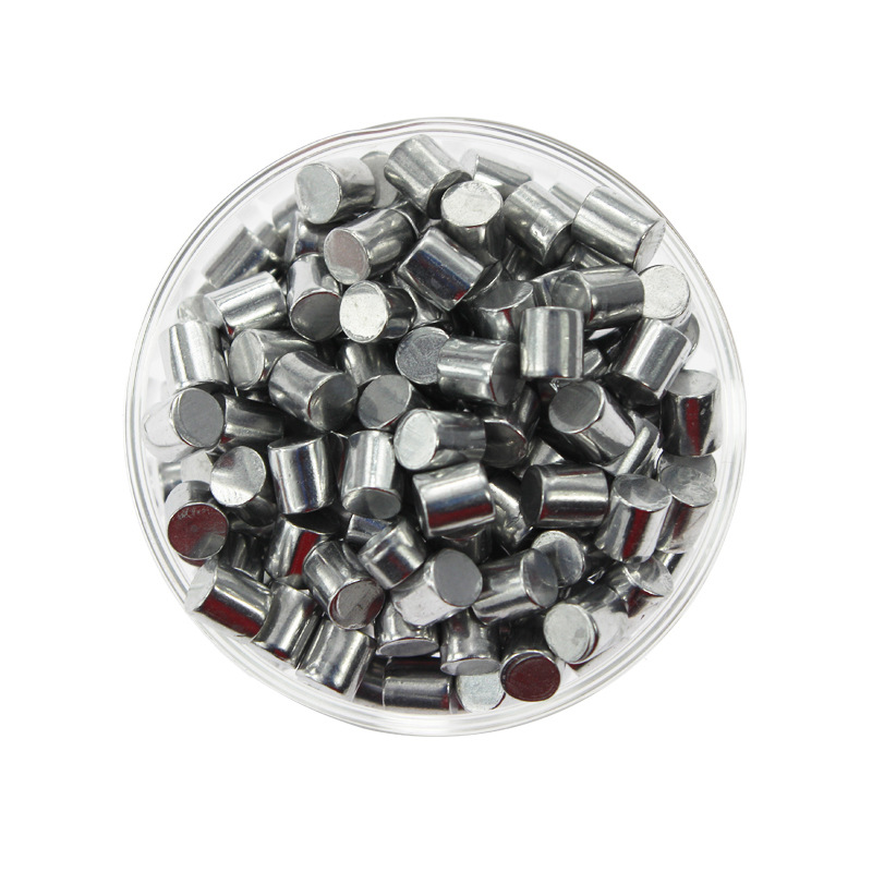

Al Aluminium Pellets Rods Evaporation Materials 3N – 6N5 (99.9% – 99.99995%)
$10.00 – $499.00Select options This product has multiple variants. The options may be chosen on the product page -