Substrates - Tinsan Materials")


 Substrate - Tinsan Materials")
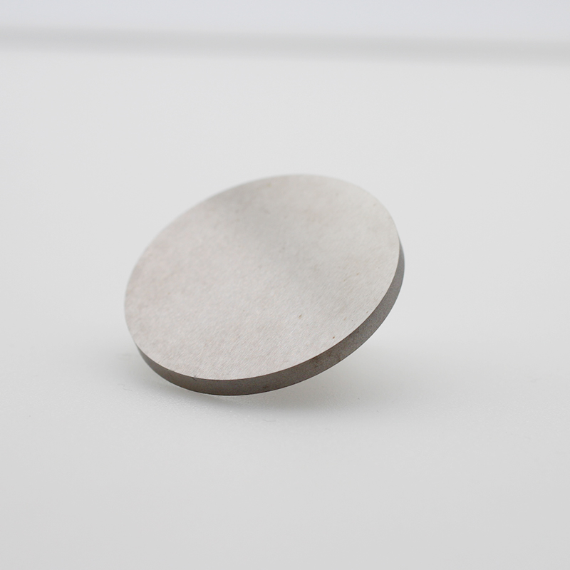
Silicon Carbide (SiC) Substrates
- Wide bandgap (3.2 eV for 4H-SiC)
- High thermal conductivity (~4.9 W/cm·K)
- Excellent chemical resistance
- High voltage breakdown strength
- Radiation hardness
- Suitable for GaN-on-SiC and epitaxial SiC device growth
Custom products or bulk orders, please contact us for competitive pricing!
- Satisfaction Guaranteed
- No Hassle Refunds
- Secure Payments
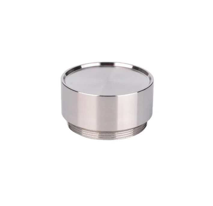
Description
Silicon Carbide (SiC) substrates are wide-bandgap semiconductor materials known for their exceptional thermal conductivity, high breakdown electric field, high saturation electron velocity, and chemical stability. These properties make SiC the ideal substrate for next-generation power electronics, RF devices, LEDs, and quantum applications operating in high-temperature, high-voltage, and high-frequency environments.
We provide high-purity single crystal SiC substrates in both 4H-SiC and 6H-SiC polytypes, with various doping types, orientations, and diameters to meet specific device fabrication needs.
Key Features:
- Wide bandgap (3.2 eV for 4H-SiC)
- High thermal conductivity (~4.9 W/cm·K)
- Excellent chemical resistance
- High voltage breakdown strength
- Radiation hardness
- Suitable for GaN-on-SiC and epitaxial SiC device growth
Specifications & Properties:
| Material | Monocrystalline Silicon Carbide (SiC) |
| Polytype | 4H-SiC or 6H-SiC |
| Conductivity Type | N-type, Semi-insulating, P-type |
| Crystal Orientation | (0001), (11-20), (1-100) |
| Diameter | 2”, 3”, 4”, 6” (custom sizes on request) |
| Thickness | 250μm – 650μm (depending on diameter) |
| Surface Finish | DSP (Double Side Polished), SSP (Single Side Polished) |
| Surface Roughness | < 0.5nm (AFM, on epi-ready polished side) |
| Off-Axis Angle | 0°, 4°, 8° (typical for epitaxy) |
| Resistivity | 0.015-0.028 Ω·cm (N-type); >10⁶ Ω·cm (SI type) |
| Micropipe Density | < 1cm⁻² or Zero MP (High-grade) |
| TTV/Bow/Warp | < 10μm (depending on diameter) |
Each wafer meets rigorous flatness, orientation, and purity requirements suitable for epitaxial processes and device fabrication.
Crystal Orientations & Grades:
① 4H-SiC (Hexagonal)
- Bandgap: 3.23 eV
- Mobility: Higher electron mobility vs 6H
- Use: Preferred for high-power, high-efficiency MOSFETs and Schottky diodes
② 6H-SiC (Hexagonal)
- Bandgap: 3.0 eV
- Use: Historically used in RF and optoelectronics
③ Conductivity Options:
- N-type (doped with N): For high-performance power devices
- Semi-insulating (compensated with vanadium): Ideal for RF devices and isolating layers
- P-type (doped with Al/B): Less common, but used in specific bipolar devices
④ Orientation Options:
- (0001) Si-face: Most commonly used for device epitaxy
- (000-1) C-face: Less common, specific epitaxy applications
- Off-axis angles: Typically 4° or 8° for step-flow growth in epitaxy
Key Advantages:
- High Breakdown Electric Field (~3 MV/cm) – Ideal for high-voltage applications
- Excellent Thermal Conductivity (~4.9 W/cm·K) – Better than GaN, supports high-power operation
- Wide Bandgap (3.2 eV for 4H-SiC) – Enables high-temperature and high-frequency performance
- Radiation Hardness – Suitable for aerospace and nuclear environments
- Mature Wafer Technology – Available up to 6” for scalable production
- Stable Crystal Structure – Enables consistent, high-yield epitaxial growth
Applications:
- Power Electronics: MOSFETs, Schottky diodes, IGBTs, JFETs for electric vehicles (EV), solar inverters, smart grids.
- RF & Microwave Devices: High-frequency amplifiers (L-band, X-band), GaN-on-SiC HEMTs for 5G, radar systems.
- LEDs & Optoelectronics: Blue and UV LEDs, SiC-based photodetectors.
- Quantum Technology: Single-photon sources and quantum sensing using defect centers (like NV centers in SiC).
- Harsh Environment Sensors: Temperature and pressure sensors in aerospace, automotive, and oil drilling environments.
- Substrate for Epitaxial Growth: High-quality epitaxy of SiC and GaN films on low-defect-density SiC substrates.
Customization Options:
We offer full customization to support R&D or mass production:
- Size Options: 2″, 3″, 4″, 6″ wafers – sliced or as-cut available
- Polytypes: 4H-SiC and 6H-SiC
- Orientation: (0001), (1-100), (11-20); Off-axis 0°, 4°, 8°
- Surface Finishing: Epi-ready polish, laser-marking, or etched flat
- Doping: N-type (N), Semi-insulating (V), P-type (Al)
- Micropipe Control: Standard (<1 cm²) and Zero MP available
- Backside Options: Etched, polished, roughened
- Quality Grades: R&D grade, commercial grade, prime-grade for epitaxy
All substrates can be packaged in class 100 cleanroom conditions for contamination-free delivery.
Quality & Certifications
We ensure uncompromising quality and reliability through:
- XRD Rocking Curve Testing – Verifies crystal quality and orientation
- AFM Surface Characterization – Atomic-level flatness and roughness testing
- Micropipe & Defect Density Inspection – Including KOH etching, optical analysis
- Resistivity & Thickness Uniformity – Mapping across wafer surface
- ISO 9001 Certified manufacturing
- RoHS & REACH Compliant
- SEMI Standard Compliance for bow, warp, TTV, edge chipping
Ordering & Contact Information:
We offer flexible MOQ (Minimum Order Quantity), competitive pricing and global delivery. For custom orders or technical inquiries, please contact us for a detailed consultation!