Substrates - Tinsan Materials")

 Substrate - Tinsan Materials")
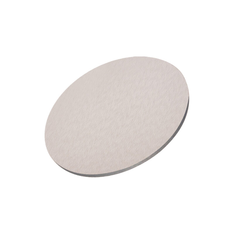
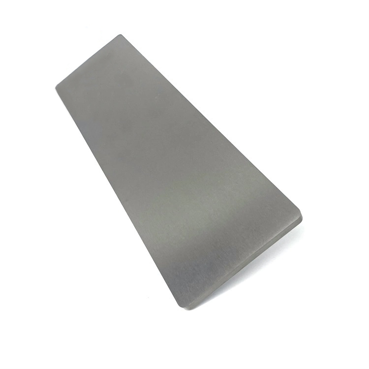
Strontium Titanate (SrTiO3) Substrates
- Perfect cubic structure at room temperature
- High dielectric constant (~300 at room temperature)
- Low loss tangent
- Excellent lattice match with perovskite oxides (e.g., YBCO, LSMO, BST)
- High optical transparency in the visible and near-infrared range
- Atomically flat surfaces achievable after polishing
Custom products or bulk orders, please contact us for competitive pricing!
- Satisfaction Guaranteed
- No Hassle Refunds
- Secure Payments
Description
Strontium Titanate (SrTiO₃, STO) is a perovskite-structured oxide crystal widely used as a substrate material for growing various thin films, especially in oxide electronics, high-temperature superconductors, ferroelectric materials, and photonic devices.
Its excellent lattice matching with many perovskite oxides, high dielectric constant, and atomically flat surface after polishing make it the ideal platform for epitaxial growth and advanced functional materials research.
Key Features:
- Perfect cubic structure at room temperature
- High dielectric constant (~300 at room temperature)
- Low loss tangent
- Excellent lattice match with perovskite oxides (e.g., YBCO, LSMO, BST)
- High optical transparency in the visible and near-infrared range
- Atomically flat surfaces achievable after polishing
Specifications & Properties:
| Material | Single Crystal Strontium Titanate (SrTiO₃) |
| Crystal Structure | Cubic perovskite (Pm3m) at room temperature |
| Lattice Constant | 3.905 Å |
| Orientation | <100>, <110>, <111> (other orientations customizable) |
| Size | 5×5 mm², 10×10 mm², 20×20 mm², 1”, 2” diameter, custom |
| Thickness | 0.5 mm, 1.0 mm, custom thickness available |
| Surface Finish | Single-side polished (SSP) or Double-side polished (DSP) |
| Surface Roughness (Ra) | < 0.5nm (AFM) on polished side |
| Mosaic Spread | < 0.1° |
| Dielectric Constant (εr) | ~300 (at room temperature) |
| TTV (Total Thickness Variation) | < 10μm |
| Crystallographic Quality | Dislocation-free, atomically smooth, high-purity |
Crystal Orientations & Grades:
- Common Orientations:
- <100>: Most commonly used, standard square lattice for perovskite epitaxy
- <110>: Provides anisotropic surface structures
- <111>: Offers a denser atomic plane for specific epitaxial applications
- Grades Available:
- Research Grade: Excellent for R&D, prototyping, and experimental deposition
- Production Grade: Tight specifications for batch production and thin-film manufacturing
- Epi-Ready Grade: Chemically cleaned and polished for immediate epitaxy use
Key Advantages:
- Lattice Match Excellence – Ideal match to perovskite oxide thin films
- High Dielectric Constant – Enables RF devices, capacitors, tunable devices
- Atomically Smooth Surface – Supports layer-by-layer epitaxial film growth
- Optical Transparency – Suitable for photonics and optoelectronic applications
- Stable Cubic Phase – Maintains symmetry across a wide temperature range
- Low Defect Density – Facilitates high-performance device fabrication
Applications:
- High-Temperature Superconductors (HTS): Epitaxial growth of YBa₂Cu₃O₇₋ₓ (YBCO) superconducting films.
- Ferroelectric Thin Films: Deposition of BaTiO₃ (BTO), Pb(Zr,Ti)O₃ (PZT) for non-volatile memory and sensors.
- Oxide Electronics: Platform for LaAlO₃/SrTiO₃ heterostructures, 2D electron gas (2DEG) studies.
- Photonic Devices: SrTiO₃ substrates for tunable optical components due to high εr.
- Microwave and RF Devices: Fabrication of tunable filters, phase shifters, and capacitors.
- Quantum Research: Surface studies on SrTiO₃ for quantum materials, interface engineering, and spintronics.
Customization Options:
We support complete customization based on your project or production requirements:
- Size Options: 5×5 mm², 10×10 mm², 20×20 mm², Ø1”, Ø2”, and custom dimensions.
- Thickness Options: 0.5 mm, 1.0 mm, custom thickness for epitaxy or mechanical stability.
- Orientation Options: <100>, <110>, <111>, and other specific cuts upon request.
- Polish Options: Single side polished (SSP) or double side polished (DSP).
- Surface Quality: Epi-ready polishing, chemical cleaning, low TTV and bow specifications.
- Special Treatments: Atomically flat (step-terrace) surface preparation available.
- Packaging: Cleanroom class 100 packaging, individually packed or in wafer carriers.
Quality & Certifications:
We maintain stringent quality control and international standards:
- X-ray Diffraction (XRD) Testing: Confirm crystal structure and orientation accuracy
- Atomic Force Microscopy (AFM): Check surface roughness and atomic step terraces
- Laue Back Reflection: Orientation verification
- Optical Inspection: Scratch and particle free
- ISO 9001 Certified production facilities
- RoHS and REACH Compliant
- SEMI Standard Packaging and handling procedures
Ordering & Contact Information:
We offer flexible MOQ (Minimum Order Quantity) and competitive pricing. Our substrates are packaged in Class 100 cleanroom environments and shipped worldwide. For custom orders or technical inquiries, please contact us for a detailed consultation!