 Single Crystal Substrates - Tinsan Materials")
 Single Crystals - Tinsan Materials")
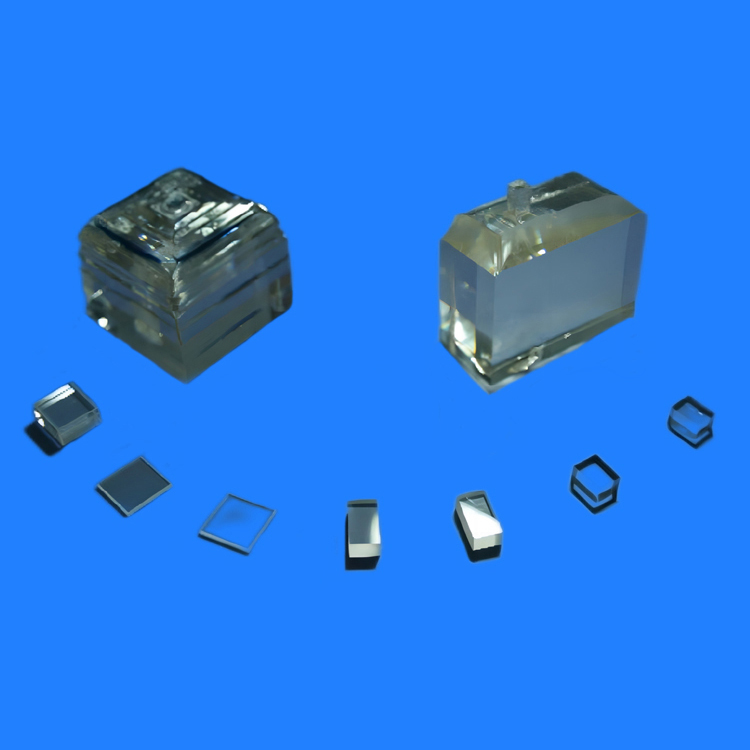
Yttrium Aluminum Oxide (YAlO3, YAP) Single Crystal Substrates
- High Thermal Stability: Suitable for high-temperature environments and laser operations.
- Excellent Mechanical Strength: Durable and resistant to cracking during processing.
- Broad Optical Transparency: Ranging from ~230 nm to 5.5 μm.
- Low Thermal Expansion Coefficient: Reduces thermal stress during device fabrication.
- High Refractive Index: Beneficial for optical and laser device efficiency.
- Good Chemical Resistance: Stable against most acids and alkalis under normal conditions.
- Low Dielectric Loss: Suitable for microwave and RF applications.
- Efficient Host Crystal: Ideal for rare-earth doping for laser crystals (e.g., Nd:YAP lasers).
Custom products or bulk orders, please contact us for competitive pricing!
- Satisfaction Guaranteed
- No Hassle Refunds
- Secure Payments
Description
Yttrium Aluminum Oxide (YAlO₃, commonly referred to as YAP) single crystal substrates are highly valued in laser, optoelectronic, and photonic applications due to their excellent thermal stability, mechanical strength, and optical transparency.
YAP substrates serve as an ideal host material for doping with rare-earth ions (such as Nd³⁺, Er³⁺, or Yb³⁺) to fabricate solid-state lasers and scintillator devices. Their close lattice match with various epitaxial layers also makes them suitable for thin film growth.
We offer high-quality YAP single crystal substrates with customizable orientations, sizes, and surface finishes to meet the demanding needs of advanced applications.
Crystal Structure and Orientation:
- Chemical Formula: YAlO₃
- Crystal Structure: Orthorhombic
- Space Group: Pnma
- Lattice Constants:
- a = 5.179 Å
- b = 5.307 Å
- c = 7.355 Å
- Density: ~5.35 g/cm³
- Melting Point: ~1875°C
- Refractive Index: ~1.93 at 550 nm
- Available Orientations:
- (100), (010), (001) planes
- Custom orientations based on specific application requirements
Key Properties and Advantages:
- High Thermal Stability: Suitable for high-temperature environments and laser operations.
- Excellent Mechanical Strength: Durable and resistant to cracking during processing.
- Broad Optical Transparency: Ranging from ~230 nm to 5.5 μm.
- Low Thermal Expansion Coefficient: Reduces thermal stress during device fabrication.
- High Refractive Index: Beneficial for optical and laser device efficiency.
- Good Chemical Resistance: Stable against most acids and alkalis under normal conditions.
- Low Dielectric Loss: Suitable for microwave and RF applications.
- Efficient Host Crystal: Ideal for rare-earth doping for laser crystals (e.g., Nd:YAP lasers).
Typical Applications:
- Solid-state laser crystals (e.g., Nd:YAP lasers)
- Scintillators for medical imaging and industrial inspection
- Thin film substrates for high-performance optical coatings
- Optical isolators, modulators, and waveguides
- Nonlinear optical devices
- Research and development in photonics and optoelectronics
- Microwave and RF components
Specifications:
| Diameter | 10 mm – 50.8 mm (customizable) |
| Thickness | 0.3 mm – 2 mm |
| Orientation | (100), (010), (001), custom available |
| Surface Finish | Single-side or double-side polished |
| Surface Quality | 10-5, 20-10, or 40-20 Scratch-Dig |
| Flatness | λ/8 or better at 632.8 nm |
| Parallelism | <10 arc seconds |
| Purity | ≥99.999% (5N) YAP |
| Crystal Growth Method | Czochralski (CZ) method |
Available Sizes and Customization:
- Wafer Sizes: 10 mm, 20 mm, 25.4 mm (1 inch), 50.8 mm (2 inch), custom
- Thickness Options: 0.5 mm, 1.0 mm, 2.0 mm; customizable upon request
- Polishing:
- Single-Side Polished (SSP)
- Double-Side Polished (DSP)
- Orientation Precision: ±0.5° or better
- Edge Options: Beveled, rounded, or customized to customer needs
- Surface Roughness: ≤3 Å RMS available on request
- Special Services:
- Laser marking or notching
- Custom shapes like squares or rectangles
- Pre-coated surfaces for thin film growth
Quality Assurance:
Our YAP single crystal substrates undergo strict quality control processes, including:
- X-Ray Diffraction (XRD) and Laue back reflection analysis
- Surface roughness measurement with Atomic Force Microscopy (AFM)
- Optical transmission testing with UV-Vis-NIR spectrometers
- Interferometric measurement for flatness and parallelism
- Visual inspections for defects, inclusions, and surface damages
- Cleanroom-grade packaging (Class 1000) to prevent contamination
Why Choose Our YAlO₃ (YAP) Single Crystal Substrates?
- High-purity YAP crystals grown using advanced Czochralski techniques
- Flexible customization of sizes, orientations, and finishes
- Excellent quality control ensuring low defect density and high surface quality
- Professional technical support for laser, optical, and photonic applications
- Global logistics network offering fast and reliable delivery
- Competitive pricing without compromising on quality
Ordering & Contact Information:
We offer flexible MOQ (Minimum Order Quantity) and competitive pricing. Our substrates are packaged in Class 100 cleanroom environments and shipped worldwide. For custom orders or technical inquiries, please contact us for a detailed consultation!
Related products
-
-
-
-
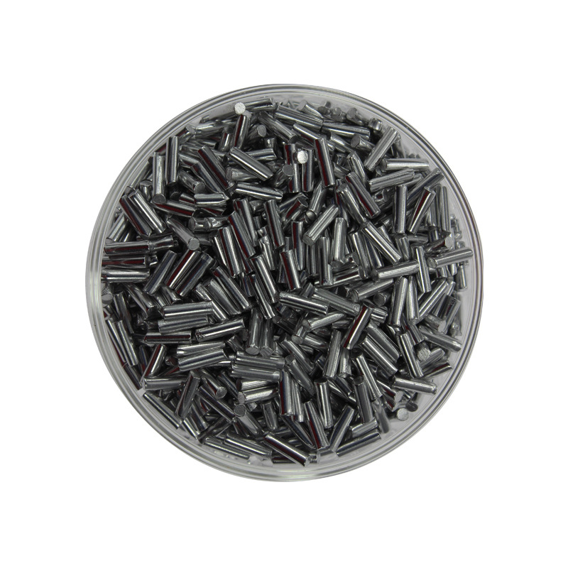
AZO (Aluminum-Doped Zinc Oxide) Pellets Granules Evaporation Materials
$40.00 – $320.00Select options This product has multiple variants. The options may be chosen on the product page
 KTN Crystal (KTa₀.₅Nb₀.₅O₃) – Orientation, 10 × 10 × 0.5 mm