Single Crystal Substrates")
Zinc Oxide (ZnO) Single Crystal Substrates
- Wide Direct Bandgap: 3.37 eV at room temperature
- High Exciton Binding Energy: ~60 meV, suitable for UV optoelectronics
- Excellent Lattice Match: Compatible with GaN, AlN, and ZnMgO film growth
- High Optical Transparency: From UV to near-IR regions
- Strong Piezoelectric Effect: Ideal for SAW and bulk acoustic wave devices
- Low Dislocation Density: <10⁴ cm⁻² (typical hydrothermal-grown crystal)
- Thermal & Chemical Stability: Stable under high temperature and various process conditions
- Multiple Orientations Available: (0001), (10-10), (11-20), etc.
-
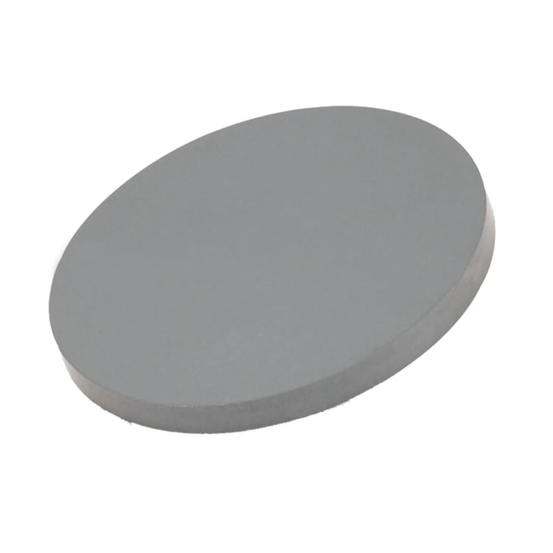
Epi-Ready Polished Surfaces: Double-side polished (DSP) with ultra-flat surface
Custom products or bulk orders, please contact us for competitive pricing!
- Satisfaction Guaranteed
- No Hassle Refunds
- Secure Payments
Description
Zinc Oxide (ZnO) single crystal substrates are wide-bandgap semiconductor materials known for their excellent optical, electrical, and piezoelectric properties. ZnO substrates provide an ideal lattice match for epitaxial growth of GaN, AlN, and other III-nitride or oxide-based thin films. With a direct bandgap of ~3.37 eV and high exciton binding energy (~60 meV), ZnO is widely used in optoelectronic devices such as LEDs, laser diodes, transparent conductive oxides, and UV photodetectors.
Our ZnO substrates are grown using hydrothermal or vapor-phase transport (VPT) methods, ensuring high crystalline quality, low dislocation density, and uniform surface morphology suitable for high-end epitaxial and device applications.
Key Features and Properties:
- Wide Direct Bandgap: 3.37 eV at room temperature
- High Exciton Binding Energy: ~60 meV, suitable for UV optoelectronics
- Excellent Lattice Match: Compatible with GaN, AlN, and ZnMgO film growth
- High Optical Transparency: From UV to near-IR regions
- Strong Piezoelectric Effect: Ideal for SAW and bulk acoustic wave devices
- Low Dislocation Density: <10⁴ cm⁻² (typical hydrothermal-grown crystal)
- Thermal & Chemical Stability: Stable under high temperature and various process conditions
- Multiple Orientations Available: (0001), (10-10), (11-20), etc.
-
Epi-Ready Polished Surfaces: Double-side polished (DSP) with ultra-flat surface
Typical Applications:
- Epitaxial templates for GaN, AlN, ZnMgO, or InGaN thin films
- UV LEDs and laser diodes
- Transparent conductive oxide (TCO) layers
- Surface acoustic wave (SAW) devices and bulk acoustic wave (BAW) resonators
- UV and visible photodetectors
- Piezoelectric and pyroelectric sensors
- High-frequency acoustic devices
- Thin-film transistors (TFTs) and oxide electronics
Material Properties and Crystal Structure:
| Material | Zinc Oxide (ZnO) |
| Crystal Structure | Wurtzite (Hexagonal) |
| Space Group | P6₃mc |
| Lattice Constants | a = 3.249 Å, c = 5.206 Å |
| Density | 5.606 g/cm³ |
| Bandgap | 3.37 eV (Direct) |
| Exciton Binding Energy | 60 meV |
| Refractive Index (633 nm) | ~2.0 |
| Thermal Conductivity | 0.6-1.2 W/cm·K |
| Thermal Expansion | αₐ = 4.75×10⁻⁶ K⁻¹, α𝑐 = 2.9×10⁻⁶ K⁻¹ |
| Hardness (Mohs) | ~4.5 |
| Transparency Range | 360 nm – 4500 nm |
| Typical Orientations | (0001), (10-10), (11-20) |
| Surface Finish | DSP (Double-Side Polished) |
| Orientation Accuracy | ±0.5° |
| Surface Quality | 10-5 or better (Scratch/Dig) |
| Standard Sizes | 10×10 mm², 20×20 mm², 10×5×0.5 mm, 5×5×0.5 mm, Ø1”, Ø2”, customized |
| Applications | GaN/AlN epitaxy, SAW/BAW devices, UV detectors, piezoelectric sensors |
Customization Options:
- Orientation: (0001), (10-10), (11-20), (000-1)
- Size: 5×5 mm² up to 2-inch diameter
- Thickness: 0.3–2 mm
- Surface Finish: SSP (single-side polished) or DSP (double-side polished)
- Surface Quality: <10-5 Scratch-Dig (MIL-PRF-13830B standard)
- Coatings: Optional AR or conductive coatings
- Orientation Accuracy: ±0.5°
- Epi-ready polishing and cleaning process available
Packaging and Delivery:
- Cleanroom packaging with Class 100 standard
- Moisture-proof, anti-static vacuum-sealed wrapping
- Double protection against mechanical shock
- Standard delivery time: 3–4 weeks (custom orders: 4–6 weeks)
- Accompanied with quality inspection report including XRD, orientation, and surface roughness data
Why Choose Us:
- Over a decade of crystal growth and wafer processing experience
- Hydrothermal-grown ZnO crystals with superior crystalline perfection
- Strict quality inspection: XRD rocking curve < 50 arcsec
- ISO-certified polishing and surface preparation facilities
- Reliable customization service for advanced optoelectronic research and production
- Trusted by academic institutions and semiconductor manufacturers worldwide
Ordering & Contact Information:
We offer flexible MOQ (Minimum Order Quantity) and competitive pricing. Our substrates are packaged in Class 100 cleanroom environments and shipped worldwide. For custom orders or technical inquiries, please contact us for a detailed consultation!