 Single Crystal Substrates - Tinsan Materials")
 Single Crystal Substrates - Tinsan Materials")
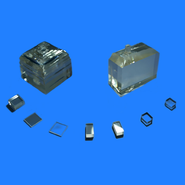
KTN (Potassium Tantalate Niobate, KTa₁₋ₓNbₓO₃) Single Crystal Substrates
- Exceptional Electro-Optic Performance: Extremely high electro-optic coefficients enabling high-speed modulation and tunable devices.
- High Dielectric Constant: Useful for applications in capacitors and tunable microwave devices.
- Wide Transparency Range: Optical transmission from near-UV (~400 nm) to mid-IR (~5.5 μm).
- Tunable Refractive Index: Ability to electrically modulate optical properties.
- Low Optical Absorption: High transmission and low loss across the IR and visible spectrum.
- Precise Composition Control: Customizable Nb/Ta ratios (x values) to tailor ferroelectric and optical properties.
- Good Chemical Stability: Suitable for long-term operation in standard laboratory environments.
Custom products or bulk orders, please contact us for competitive pricing!
- Satisfaction Guaranteed
- No Hassle Refunds
- Secure Payments
Description
KTN (Potassium Tantalate Niobate, KTa₁₋ₓNbₓO₃) single crystal substrates are advanced ferroelectric and electro-optic materials characterized by extremely high dielectric constants, significant electro-optic coefficients, and strong nonlinear optical properties. These features make KTN substrates ideal for applications in tunable optics, high-speed modulators, infrared detectors, and quantum photonics. Our high-quality KTN crystals offer excellent compositional control, superior homogeneity, and surface quality for demanding research and industrial applications.
Key Features and Properties:
- Exceptional Electro-Optic Performance: Extremely high electro-optic coefficients enabling high-speed modulation and tunable devices.
- High Dielectric Constant: Useful for applications in capacitors and tunable microwave devices.
- Wide Transparency Range: Optical transmission from near-UV (~400 nm) to mid-IR (~5.5 μm).
- Tunable Refractive Index: Ability to electrically modulate optical properties.
- Low Optical Absorption: High transmission and low loss across the IR and visible spectrum.
- Precise Composition Control: Customizable Nb/Ta ratios (x values) to tailor ferroelectric and optical properties.
- Good Chemical Stability: Suitable for long-term operation in standard laboratory environments.
Typical Applications:
- Tunable laser modulators
- Electro-optic Q-switches
- IR phase shifters and spatial light modulators (SLMs)
- High-speed optical communications devices
- Quantum optics and quantum information systems
- Ferroelectric memory devices
- Terahertz wave generation and detection
- Nonlinear optical components
Specifications:
| Chemical Formula | KTa₁₋ₓNbₓO₃ (0 < x < 1) |
| Crystal Structure | Cubic perovskite (Pm3m) |
| Lattice Constant | ~3.99-4.01 Å |
| Density | ~7.03 g/cm³ |
| Curie Temperature | 40-300 K (depending on composition) |
| Dielectric Constant | >10⁴ near Curie temperature |
| Electro-optic Coefficient | Very high (r₃₃ > several hundred pm/V) |
| Optical Transmission Range | 400 nm – 5.5 μm |
| Refractive Index (at 1.5 μm) | ~2.2 |
| Surface Quality | 20/10 (Scratch/Dig) |
| Surface Flatness | <λ/10 @ 632.8 nm |
| Available Orientations | (100), (110), (111) |
| Typical Sizes | 5×5 mm², 10×10 mm², 20×20 mm² |
| Thickness Range | 0.5 mm – 2.0 mm |
| Surface Finish | SSP or DSP |
Material Properties and Crystal Structure:
- Chemical Formula: KTa₁₋ₓNbₓO₃ (0 < x < 1)
- Crystal Structure: Perovskite-type cubic structure (above Curie temperature)
- Space Group: Pm3m (cubic)
- Lattice Constant: ~3.99–4.01 Å (depending on x)
- Density: ~7.03 g/cm³
- Curie Temperature: Typically between 40–300 K (composition-dependent)
- Optical Transmission Range: 400 nm – 5.5 μm
- Refractive Index: ~2.2 at 1.5 μm
- Electro-optic Coefficient: Extremely high (r₃₃ > several hundred pm/V)
- Dielectric Constant: >10⁴ at Curie temperature (for certain compositions)
Standard Product Sizes and Availability:
- Standard wafer sizes: 5×5 mm², 10×10 mm², 20×20 mm²
- Thickness range: 0.5 mm to 2.0 mm (customizable)
- Surface Finishing: Single Side Polished (SSP) or Double Side Polished (DSP)
- Orientation: (100), (110), (111) available
- Surface Quality: 20/10 or better (MIL-PRF-13830B standard)
- Surface Flatness: <λ/10 at 632.8 nm
- Edge treatment: Sawn, ground, or beveled upon request
- Nb concentration (x value): customizable upon request (e.g., x=0.3, 0.5, 0.7)
Customization Options:
- Precise doping levels and compositional control (custom x value)
- Custom orientation, size, and thickness
- Surface polishing grade adjustments for specific optical requirements
- AR (Anti-Reflection) coatings available for specific laser wavelengths
- Ultra-low birefringence finishing options
- Custom packaging for ultra-high cleanliness and moisture-sensitive applications
Packaging and Delivery:
- Packaged in Class 100 cleanroom environment
- Vacuum-sealed to prevent contamination and moisture absorption
- Desiccant included to maintain low humidity
- Standard lead time: 2–4 weeks for stock items; custom orders upon request
- Inspection Reports: Orientation, thickness, surface quality, and XRD data available
Why Choose Our KTN (Potassium Tantalate Niobate, KTa₁₋ₓNbₓO₃) Single Crystal Substrates?
- In-house crystal growth technology with precise compositional control
- High optical quality with minimal defects and inclusions
- Advanced polishing techniques to achieve ultra-smooth surfaces
- Full customization service to match application-specific requirements
- Competitive lead times and consistent product quality
- Comprehensive technical support and after-sales services
Ordering & Contact Information:
We offer flexible MOQ (Minimum Order Quantity) and competitive pricing. Our substrates are packaged in Class 100 cleanroom environments and shipped worldwide. For custom orders or technical inquiries, please contact us for a detailed consultation!

 KTN Crystal (KTa₀.₅Nb₀.₅O₃) – Orientation, 10 × 10 × 0.5 mm