Showing 361–372 of 686 results
-
- Corrosion Resistance: Excellent performance in seawater, acidic, and alkaline environments.
- High Strength: Maintains structural integrity under stress and extreme conditions.
- Versatile Fabrication: Ideal for welding, machining, and advanced manufacturing techniques.
- Thermal Stability: Performs reliably at both low and high temperatures.
- Non-Magnetic: Retains non-magnetic properties in various conditions.
-
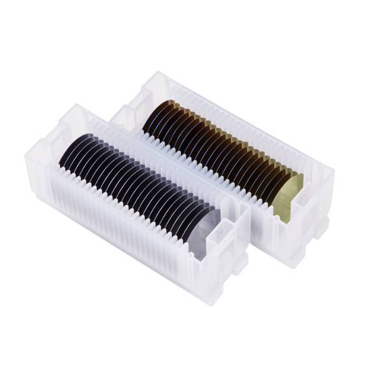

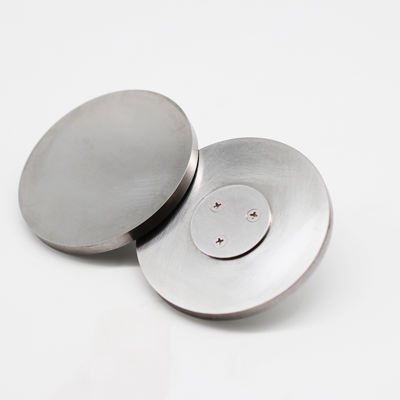
- Diameter Choices: 2″ to 12″ (or custom sizes).
- Doping Concentration: Custom doping profiles for N-type and P-type wafers.
- Thickness Variability: From ultra-thin wafers to thick substrates.
- Crystal Orientation: Standard orientations include <100>, <111>, <110>, with custom orientations available.
- Flat & Edge Treatment: Rounded, chamfered, or custom edge profiles.
- Surface Finishing:
- SSP (Single-Side Polished) or DSP (Double-Side Polished).
- Oxide coating, etched surfaces, or epitaxial layers upon request.
-
- High Purity: Guarantees superior film quality and reduces impurities.
- Excellent Conductivity: Suitable for applications requiring conductive thin films.
- Thermal Stability: Performs reliably in high-temperature environments.
- Customizable Specifications: Tailored to specific sputtering system requirements.
- Versatility: Compatible with various sputtering techniques, including RF and DC.
-
- High Optical Transparency: MoO₃ is transparent in the visible spectrum and is often used in optoelectronic devices that require high transparency and conductivity.
- Excellent Electrical Conductivity: MoO₃ is often used to improve charge injection in electronic devices, particularly in organic electronic applications.
- Thermal Stability: It has a high melting point (~795°C), making it suitable for high-temperature evaporation processes.
- Chemical Properties: MoO₃ is known for its oxidation properties, making it useful in catalysis and other chemical applications.
- Layer Uniformity: When used in deposition processes, MoO₃ can form highly uniform thin films with excellent adhesion properties.
-
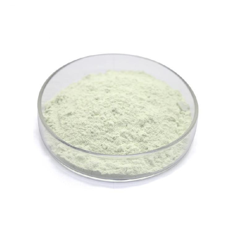
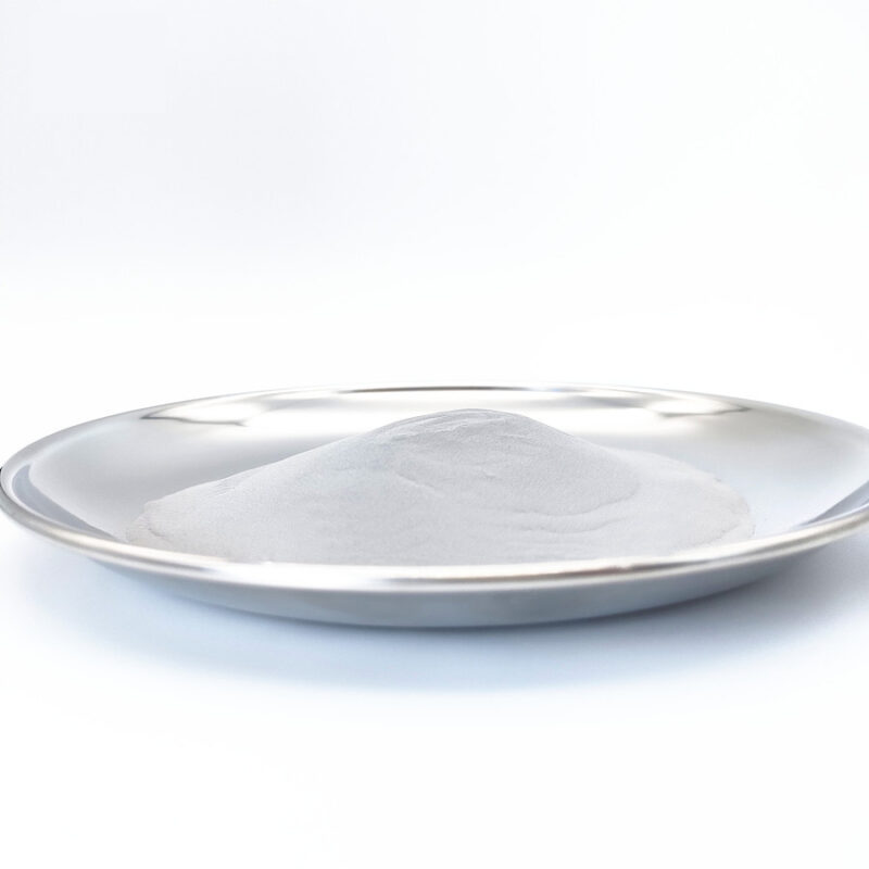
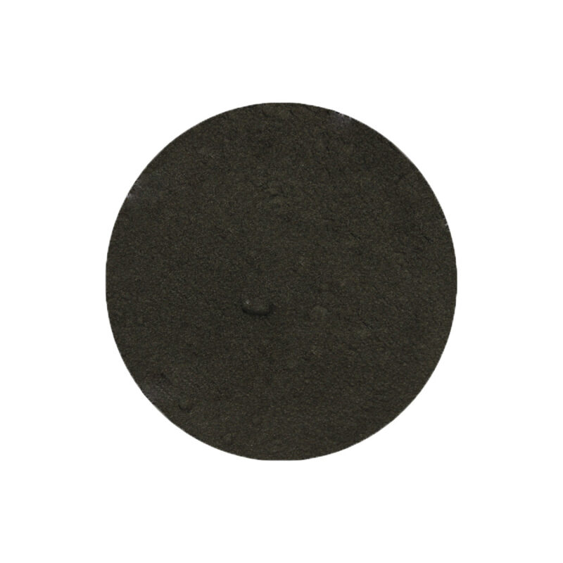
- High Purity: Ensures reliable performance in sensitive applications.
- Thermal Stability: Withstands high-temperature environments.
- Oxidizing Agent: Ideal for catalytic and chemical synthesis.
- Semiconducting Properties: Applicable in electronic devices.
- Customizable Particle Sizes: Nano to micrometer scales available.
- Excellent Optical Transparency: Suitable for optical coatings and devices.
-

- High Work Function: MoO₃ is known for its high work function, which makes it ideal for applications requiring efficient charge injection or extraction, such as OLEDs and OPVs.
- Excellent Catalytic Properties: MoO₃ is a robust catalyst, especially in oxidation reactions, making it suitable for industrial chemical processes and catalytic thin films.
- Electrochromic Behavior: MoO₃’s ability to undergo reversible oxidation-reduction reactions makes it ideal for use in electrochromic devices.
- Optical Transparency: MoO₃ thin films can be transparent in the visible and near-infrared regions, which is beneficial for optoelectronic devices requiring transparent electrodes or coatings.
-
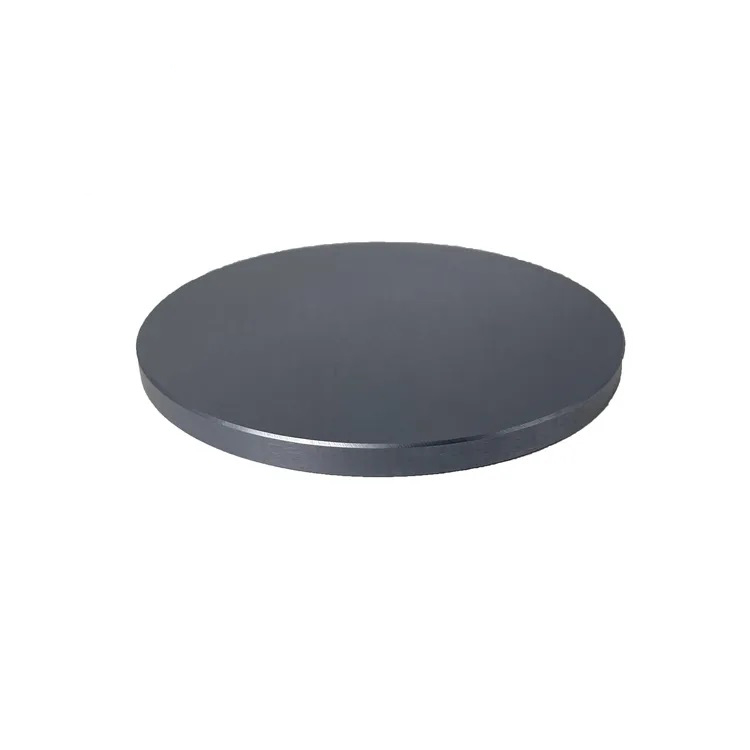
- High Thermal Stability: Performs exceptionally well in extreme temperature environments.
- Enhanced Ductility: Improved mechanical performance over pure molybdenum.
- Excellent Conductivity: Ensures reliable electrical and thermal performance.
- Customizable Options: Tailored to meet the specific requirements of various deposition systems.
- Corrosion Resistance: Long-lasting performance in aggressive environments.
-

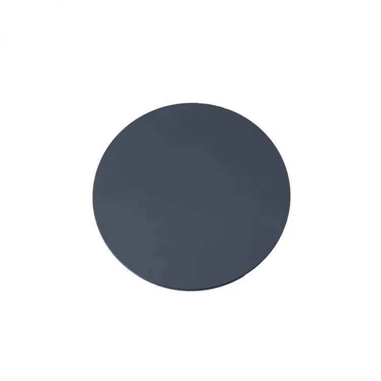
- Layered Structure: MoS₂ has a unique layered structure, allowing for exfoliation into single or few layers, making it ideal for 2D material applications.
- Semiconductor Properties: MoS₂ is a semiconductor with a direct bandgap (~1.8 eV for monolayers), making it suitable for nanoscale transistors and photodetectors.
- Low Friction Coefficient: Its excellent lubrication properties make MoS₂ ideal for coatings that require low friction and high durability, especially in vacuum or extreme conditions.
- Thermal Stability: MoS₂ remains stable at high temperatures, ensuring its effectiveness in harsh environments.
- Corrosion Resistance: MoS₂ provides a protective, corrosion-resistant layer in various applications, extending the life of coated components.
-
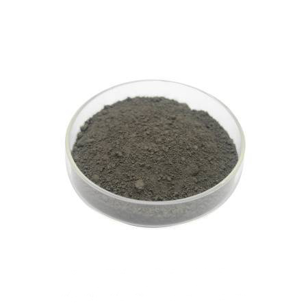
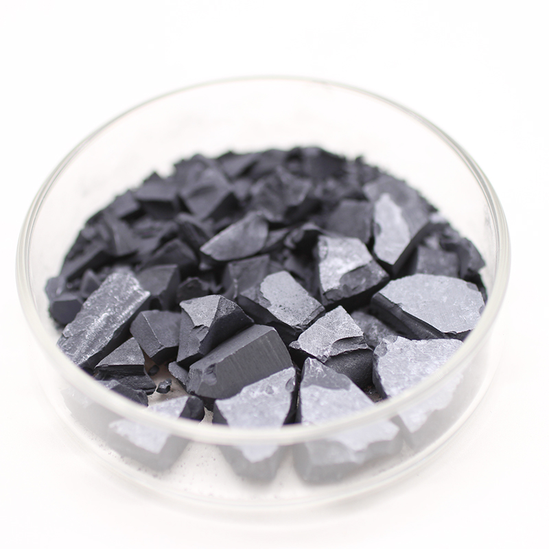
- Superior Lubrication: Known for its excellent lubrication properties, particularly in extreme temperature and pressure environments.
- High Wear Resistance: Provides exceptional wear protection and reduces friction in moving parts.
- Thermal Stability: Maintains stability at high temperatures, making it suitable for demanding industrial environments.
- Good Conductivity: Possesses moderate electrical conductivity, making it useful in electrical applications.
- Chemical Resistance: Highly resistant to oxidation and corrosion, making it durable in harsh chemical environments.
- Fine Powder Form: Available in various particle sizes, offering flexibility for different applications.
-

- Layered Structure: MoS2 has a unique layered structure that contributes to its mechanical, electrical, and tribological properties, making it an excellent candidate for advanced coatings and devices.
- Semiconducting Properties: MoS2 is a semiconductor with a direct bandgap in its monolayer form, offering high performance in electronic devices such as transistors and photodetectors.
- Low Friction Coefficient: As a solid lubricant, MoS2 provides a low friction coefficient, making it useful in harsh environments where liquid lubricants are impractical.
- High Thermal and Chemical Stability: MoS2 films exhibit excellent thermal and chemical stability, enabling their use in high-temperature environments and chemically aggressive conditions.
-
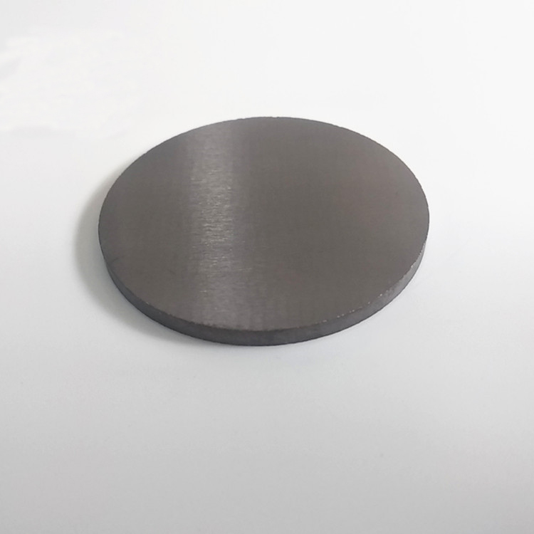

- High Purity: Ensures superior thin-film quality and device performance.
- Layered Structure: Facilitates easy exfoliation and 2D material synthesis.
- Stable Chemical Composition: Provides consistent results across various deposition processes.
- Excellent Optical and Electrical Properties: Ideal for advanced electronics and optoelectronics.
- Custom Configurations: Available in tailored sizes, shapes, and thicknesses for specific requirements.
-
- High Melting Point: Excellent stability at temperatures up to 1900°C.
- Superior Oxidation Resistance: Forms a protective silica (SiO₂) layer at high temperatures.
- Good Electrical Conductivity: Suitable for heating element production.
- Corrosion Resistance: Performs well in oxidative and corrosive environments.
- Low Density: Lightweight yet durable for advanced material designs.