Showing 421–432 of 686 results
-
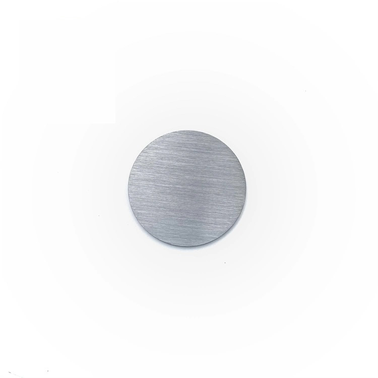
- Low Resistivity: NiSi₂ has excellent electrical conductivity, making it ideal for forming low-resistance contacts in silicon-based devices.
- Thermal Stability: NiSi₂ films maintain their performance at high temperatures, which is critical for high-temperature semiconductor processing.
- Good Adhesion: Thin films of NiSi₂ adhere well to silicon and other substrates, ensuring durability in semiconductor devices.
- High Purity: The high purity (typically ≥ 99.9%) of the material ensures that the deposited films have superior performance in sensitive electronic applications.
- Excellent Silicon Compatibility: NiSi₂ integrates well with silicon, which is crucial for creating stable, conductive contacts in silicon devices.
-

- Shape Memory Effect: NiTi alloys can return to their original shape after deformation when exposed to a certain temperature, making them highly valuable in applications requiring memory or actuation.
- Superelasticity: NiTi alloys exhibit significant elastic deformation, which allows them to absorb and release mechanical stress, ideal for flexible and resilient components.
- Corrosion Resistance: NiTi has excellent resistance to corrosion, making it suitable for biomedical devices and components exposed to harsh environments.
- Biocompatibility: NiTi alloys are biocompatible, making them safe for use in medical applications, particularly in implantable devices.
- Wear Resistance: The hardness and durability of NiTi alloys provide long-lasting wear resistance in protective thin films.
- Thermal Stability: NiTi films maintain their unique mechanical properties even at varying temperatures, ensuring consistent performance in diverse conditions.
-

- High Strength: NiV alloys exhibit exceptional mechanical strength, making them suitable for applications requiring durability and performance under stress.
- Corrosion Resistance: The addition of vanadium enhances the corrosion resistance of nickel, making NiV targets suitable for use in harsh environments and extending the life of thin films.
- Good Electrical Conductivity: NiV alloys maintain good electrical conductivity, which is essential for electronic and electrical applications.
- Versatility: The properties of NiV alloys can be tailored by adjusting the composition, allowing for customization to meet specific application requirements.
-
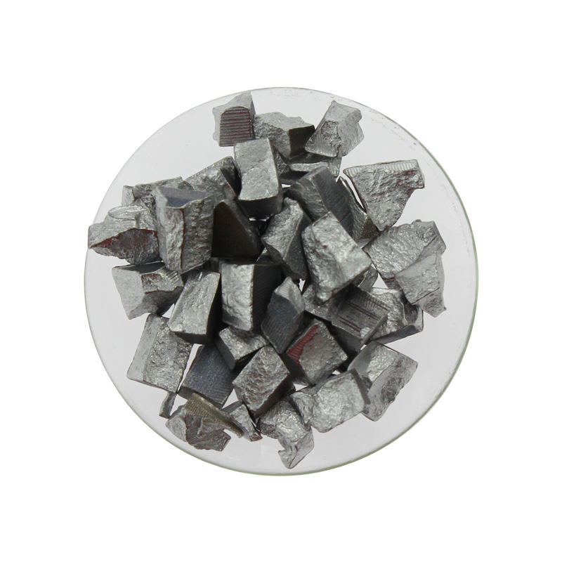
- High Strength: Offers superior tensile strength and toughness compared to standard nickel.
- Wear Resistance: Enhanced durability makes it ideal for high-friction applications.
- Corrosion Resistance: Good resistance to oxidation and chemical attack, extending the lifespan of coated components.
-

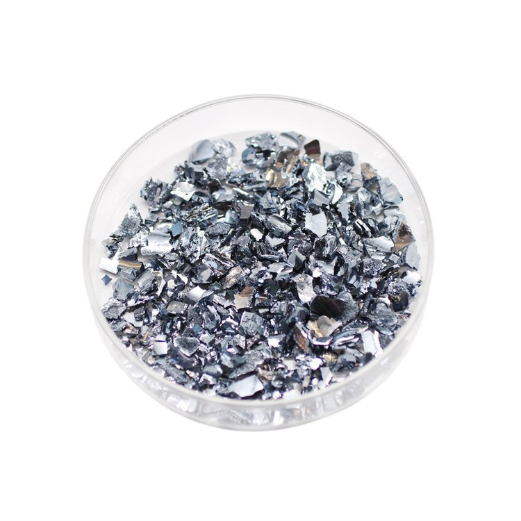
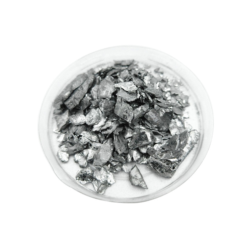
- Hardness and Durability: NiW alloys offer exceptional hardness and durability, making them ideal for wear-resistant coatings that protect mechanical parts and tools from wear and abrasion.
- Corrosion Resistance: NiW thin films provide strong resistance to corrosion, particularly in harsh environments exposed to moisture, chemicals, or high salinity, extending the service life of components.
- Thermal Stability: The alloy maintains its mechanical and chemical properties at elevated temperatures, making NiW thin films suitable for high-temperature applications in various industries.
- Magnetic Properties: The nickel content in NiW alloys provides magnetic characteristics that are useful in certain electronic and magnetic storage applications.
- Customizable Composition: The ratio of nickel to tungsten can be customized to fine-tune the properties of the thin film for specific applications, such as increasing hardness, wear resistance, or corrosion protection.
-
- High Density: Exceptional density provides effective radiation shielding.
- Malleability: Easily shaped and manipulated to fit intricate forms and surfaces.
- Corrosion Resistance: Naturally resistant to most environmental and chemical effects.
- Thermal and Acoustic Insulation: Excellent properties for heat and sound dampening.
- Durability: Withstands wear and tear in harsh environments.
- Impermeability: Blocks light, moisture, and gases, making it suitable for sensitive sealing applications.
-

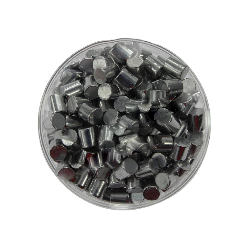
- High Purity: Typically ≥ 99.9% pure, ensuring high-quality films and minimizing impurities.
- Consistent Quality: Manufactured under controlled conditions to ensure uniformity in size and composition.
- Excellent Thermal Conductivity: Provides efficient heat transfer during the evaporation process.
- Customizable Sizes: Available in various pellet sizes to meet specific evaporation requirements.
-
- High Density: Provides superior radiation shielding and soundproofing capabilities.
- Corrosion Resistance: Stable under various environmental conditions.
- Excellent Malleability: Easily shaped for diverse industrial uses.
- Thermal and Electrical Conductivity: Suitable for conductive applications.
- Versatile Applications: Applicable in alloys, batteries, and protective coatings.
-

- Thickness: The thickness of the lead coating can be precisely controlled during the sputtering process, allowing for tailored solutions to meet specific application needs.
- Alloys: Lead sputtering targets can be produced as pure lead or in alloyed forms, such as lead-tin (Pb-Sn) or lead-silver (Pb-Ag), depending on the desired properties of the thin film.
- Backing Plates: Lead targets can be bonded to backing plates made from materials like copper or aluminum to improve thermal conductivity and mechanical stability during the sputtering process.
-
- Narrow Bandgap: PbS has a small bandgap (~0.37 eV), allowing it to detect and respond to IR radiation, making it ideal for infrared applications.
- High Infrared Sensitivity: PbS thin films exhibit excellent sensitivity to infrared light, especially in the mid-IR range, enhancing performance in IR detectors and sensors.
- Efficient Light Absorption: PbS absorbs light efficiently, making it a great material for photovoltaic devices and optoelectronic components.
- Good Thermal Stability: PbS films maintain their properties under moderate temperature conditions, suitable for use in thermal and IR-sensitive devices.
- Adaptability to Thin Films: PbS can be easily deposited as a thin film via evaporation, making it suitable for creating highly sensitive IR detectors and optical coatings.
-

- Narrow Bandgap Semiconductor: PbTe has a bandgap of approximately 0.32 eV, which enables high sensitivity to infrared radiation in the 3-5 µm range.
- High Thermoelectric Efficiency: PbTe has excellent thermoelectric properties, making it suitable for energy conversion in both power generation and refrigeration applications.
- Good Thermal and Electrical Conductivity: PbTe exhibits strong thermal and electrical conductivity, essential for efficient thermoelectric devices and IR detection systems.
- Infrared Absorption: PbTe is highly effective at absorbing infrared light, particularly in the mid-IR region, making it ideal for infrared detectors and optoelectronic devices.
- Thin Film Deposition: PbTe can be deposited as a uniform thin film through evaporation techniques, ensuring high performance in electronic and optoelectronic applications.
-
- Thermoelectric Efficiency: Exceptional thermoelectric properties for energy conversion and cooling applications.
- High Purity: ≥99.9% purity available, ensuring minimal impurities and high-quality performance.
- High Stability: Stable under both high and low temperatures, making it ideal for use in diverse temperature environments.
- Customizable Particle Size: Available in a range of particle sizes from nano to micro, suitable for various processing needs.
- Environmentally Friendly: PbTe is non-toxic and can be utilized in energy harvesting solutions, promoting sustainability.
- Versatile Application: Can be used in thermoelectric generators (TEGs) and thermoelectric coolers (TECs).