Single-Crystal Cu(111) and Ni(111) Substrates for Graphene and 2D Material Growth
The scalable growth of high-quality graphene and other two-dimensional materials depends not only on the deposition process, but also on the crystallographic structure of the substrate underneath them.
Among metallic growth substrates, single-crystal Cu(111) and Ni(111) have attracted particular attention because their close-packed (111) surfaces provide well-defined atomic arrangements for chemical vapor deposition (CVD), epitaxial growth, and fundamental surface-science studies.
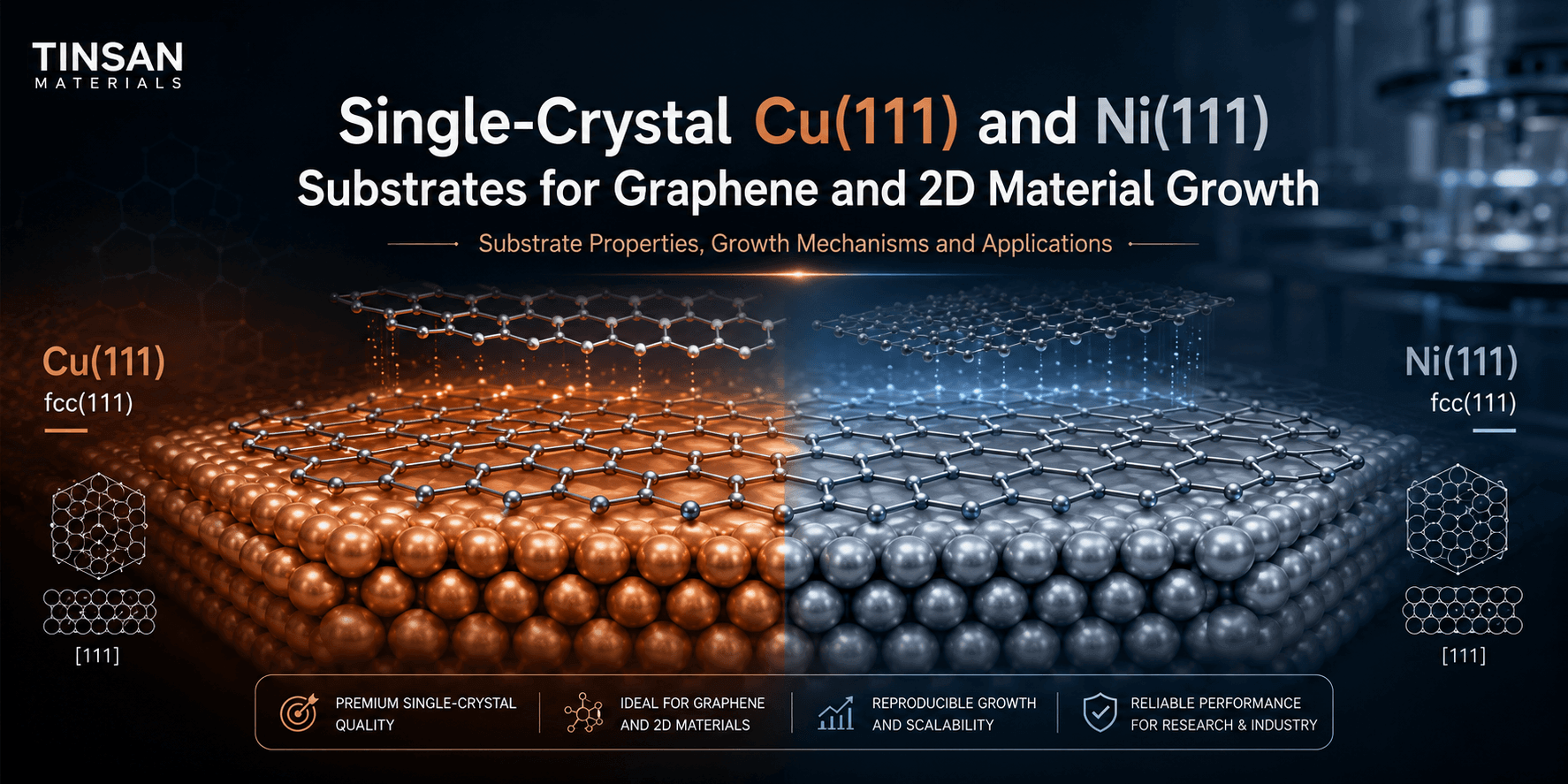
Unlike polycrystalline metal foils, which contain grains with different orientations and numerous grain boundaries, a single-crystal metal substrate offers a continuous and crystallographically uniform surface. This can improve control over nucleation, domain orientation, interfacial structure, and ultimately the quality of the deposited 2D material.
Cu(111) and Ni(111), however, are not interchangeable. Differences in lattice matching, carbon solubility, catalytic activity, and graphene–metal interaction lead to distinctly different growth behavior.
This article examines the properties of single-crystal Cu(111) and Ni(111) substrates, explains how they influence graphene growth, and discusses their expanding role in graphene, hexagonal boron nitride (hBN), and other 2D-material research.
Why Single-Crystal Metal Substrates Matter in 2D Material Growth
For epitaxial growth, the atomic arrangement of the substrate acts as a template for the material forming above it.
A polycrystalline Cu or Ni foil contains many grains. Each grain may expose a different crystallographic plane, such as (111), (100), or higher-index surfaces. Grain boundaries and local differences in surface orientation can therefore produce variations in:
A single-crystal substrate removes much of this crystallographic variability.
This becomes particularly important when individual graphene domains need to grow with the same orientation and merge without forming significant grain boundaries.
Recent research illustrates how far this concept has progressed. A 2025 Science Advances study reported 6-inch single-crystal Cu(111) wafers with a misorientation angle of approximately 0.48° and surface roughness of Ra ≈ 0.34 nm. Graphene grown on these substrates achieved an average carrier mobility of approximately 10,093 cm² V⁻¹ s⁻¹, demonstrating the connection between substrate crystallinity and wafer-scale graphene quality.
Crystal Structure of Cu(111) and Ni(111)
Both copper and nickel crystallize in the face-centered cubic (FCC) structure.
Typical room-temperature lattice constants are approximately:
| Property | Cu | Ni |
|---|---|---|
| Crystal structure | FCC | FCC |
| Bulk lattice constant | ~3.615 Å | ~3.524 Å |
| (111) surface atomic spacing | ~2.56 Å | ~2.49 Å |
| Graphene lattice constant | ~2.46 Å | ~2.46 Å |
| Approx. graphene/substrate mismatch | ~3.8% | ~1.2% |
The lattice constants of bulk Cu and Ni are about 3.615 and 3.524 Å respectively. Because the FCC (111) surface forms a hexagonal-like atomic arrangement, both surfaces are structurally compatible with graphene’s hexagonal lattice.
The difference becomes even more interesting at the interface.
Graphene on Cu(111) has a lattice mismatch of approximately 3.8%, whereas graphene on Ni(111) has a substantially smaller mismatch of about 1.2%.
This makes Ni(111) particularly close to a lattice-matched graphene/metal system.
But lattice matching alone does not determine which substrate is better.
Why Is Cu(111) Widely Used for Graphene Growth?
Copper has become one of the most important catalysts for CVD graphene because carbon has very low solubility in Cu.
At approximately 1000°C, one study reports carbon solubility in Cu at only around 75 ppm, compared with approximately 1.3 at.% in Ni under comparable conditions. Exact values reported in the literature vary with the thermodynamic model and experimental conditions, but the difference between Cu and Ni remains very large.
Surface-Dominated Growth on Copper
During methane-based CVD, hydrocarbon molecules decompose on the heated copper surface.
Carbon-containing species then migrate across the surface and participate in graphene nucleation and lateral growth.
Because relatively little carbon dissolves into the Cu bulk, graphene formation on copper is largely surface mediated.
Once the surface becomes covered by graphene, the catalytic Cu surface is progressively blocked from additional precursor decomposition. This behavior is one reason CVD on Cu tends to favor monolayer graphene.
The landmark 2009 Science study by Li et al. demonstrated centimeter-scale graphene growth on Cu, with the resulting films being predominantly single layer and less than 5% of the measured area containing few-layer graphene.
Why Cu(111) Instead of Randomly Oriented Copper?
The crystallographic orientation of Cu can influence the orientation and morphology of graphene domains.
Cu(111) is particularly attractive because its close-packed surface has symmetry compatible with graphene.
Research has demonstrated that graphene domain orientation, edge geometry, and thickness can be influenced by Cu crystallography. On Cu(111), graphene domains can preferentially align relative to specific substrate directions during appropriate CVD conditions.
This makes single-crystal Cu(111) attractive for research aimed at:
Graphene Growth on Ni(111): A Different Mechanism
Nickel presents a very different situation.
Although Ni(111) has excellent lattice compatibility with graphene, carbon dissolves much more readily in Ni than in Cu.
At elevated temperatures, carbon generated from hydrocarbon decomposition can enter the Ni substrate. As the sample cools and carbon solubility decreases, dissolved carbon may return toward the surface through segregation or precipitation.
Consequently, graphene formation on Ni can involve both surface processes and bulk carbon transport.
This mechanism can make graphene layer control more sensitive to:
If too much carbon is dissolved into Ni during growth, additional carbon can emerge during cooling and contribute to bilayer, few-layer, or multilayer graphene.
This is one reason monolayer thickness control can be more challenging on Ni than on Cu.
Why Is Ni(111) Still an Important Graphene Substrate?
The same characteristics that make Ni more difficult for monolayer thickness control also make single-crystal Ni(111) scientifically valuable.
First, the approximately 1.2% graphene/Ni(111) lattice mismatch allows graphene to form a nearly commensurate structure with the substrate.
Second, Ni interacts much more strongly with graphene than Cu does.
The interaction between graphene π states and Ni d orbitals can significantly modify graphene’s electronic structure. For this reason, graphene/Ni(111) has become an important model system for studying:
In other words, Cu(111) is frequently attractive when researchers want graphene that retains more of its intrinsic electronic behavior, while Ni(111) can be especially useful when the graphene–metal interface itself is the research subject.
Cu(111) vs. Ni(111): Which Is Better for Graphene Growth?
There is no universal answer because the optimum substrate depends on the objective of the experiment.
| Factor | Cu(111) | Ni(111) |
|---|---|---|
| Crystal structure | FCC | FCC |
| Graphene lattice mismatch | ~3.8% | ~1.2% |
| Carbon solubility at ~1000°C | Very low | Much higher |
| Dominant graphene growth behavior | Mainly surface mediated | Surface + dissolution/segregation |
| Monolayer control | Generally easier | More sensitive to process conditions |
| Graphene–metal interaction | Relatively weak | Strong |
| Domain orientation control | Excellent under optimized conditions | Excellent lattice registry |
| Multilayer tendency | Relatively low | Higher |
| Graphene transfer | Commonly used | Can be more challenging |
| Surface/interface studies | Excellent | Particularly valuable |
| hBN growth research | Yes | Yes |
Choose Cu(111) When:
The main objective is typically:
Choose Ni(111) When:
The project focuses more on:
Why Does the (111) Orientation Matter?
The importance of Cu(111) and Ni(111) is not simply a matter of naming a crystallographic plane.
In FCC metals, the (111) plane is a close-packed surface.
Its surface atoms form a triangular arrangement that produces a hexagonal-type symmetry compatible with many 2D materials.
Graphene also possesses a hexagonal lattice.
This symmetry relationship can reduce the number of energetically favorable graphene orientations during growth, helping domains align before they eventually merge.
However, symmetry matching does not automatically guarantee perfect graphene alignment.
First-principles calculations have shown that small graphene islands on Cu(111) can initially possess misorientations. As the domains become larger, their energetically preferred orientation can evolve toward alignment with the Cu(111) surface. One study calculated that near-alignment becomes increasingly favored as graphene islands grow to hundreds of nanometers, illustrating why low nucleation density is important for single-crystal graphene growth.
Therefore, crystal orientation works together with surface condition and growth parameters rather than acting independently.
Surface Quality Can Be as Important as Crystal Orientation
Buying a substrate labeled “Cu(111)” does not by itself guarantee identical CVD results.
For high-quality epitaxial growth, researchers should also consider several substrate specifications.
Surface Roughness
Steps, scratches, pits, and polishing damage can create preferential nucleation sites.
A smoother substrate can reduce uncontrolled nucleation and make the relationship between the 2D material and the underlying crystal structure easier to investigate.
Recent wafer-scale Cu(111) research has therefore focused heavily on combining single crystallinity with sub-nanometer surface roughness.
Orientation Accuracy
The nominal surface may be (111), but the actual surface normal can deviate slightly from the ideal crystallographic direction.
This deviation, commonly described using terms such as miscut angle or orientation tolerance, changes the density and arrangement of atomic steps.
For some experiments, these steps can affect nucleation and domain alignment.
Surface Contamination
Oxygen, hydrocarbons, polishing residue, and other contaminants may influence surface catalytic activity and graphene nucleation.
Consequently, substrate storage, cleaning, annealing, and surface preparation should be considered as part of the complete growth process.
Purity
Trace elements can modify catalytic behavior or introduce unwanted phases and surface chemistry.
For experiments involving fundamental surface science or highly controlled epitaxy, high-purity single-crystal metal substrates can therefore be advantageous.
Beyond Graphene: Cu(111) and Ni(111) for hBN and Other 2D Materials
The relevance of Cu(111) and Ni(111) extends beyond graphene.
hBN on Cu(111)
Hexagonal boron nitride is an electrically insulating 2D material frequently used together with graphene and transition-metal dichalcogenides.
A Nature study demonstrated wafer-scale single-crystal hBN monolayers on Cu(111) across a two-inch sapphire-supported Cu(111) substrate. The study found that interactions between hBN edges and Cu(111) step edges contributed to mono-oriented epitaxial growth.
hBN on Ni(111)
Ni(111) has also demonstrated significant potential.
A 2022 Nature study reported epitaxial growth of wafer-scale single-crystal trilayer hBN on Ni(111). The researchers identified a Ni₂₃B₆ interlayer forming between hBN and Ni during the process, illustrating how substrate chemistry can become part of the epitaxial growth mechanism.
These results demonstrate an important principle:
The substrate is not merely a mechanical support for a 2D film—it can actively determine nucleation, orientation, interface chemistry, and crystal quality.
Cu–Ni(111) Alloys: Combining the Advantages of Copper and Nickel
An emerging direction is to move beyond pure Cu or pure Ni and deliberately tune substrate chemistry using single-crystal Cu–Ni(111) alloys.
Adding controlled amounts of Ni to Cu increases catalytic activity and carbon solubility while retaining the crystallographic characteristics of the (111) surface.
This provides another variable for controlling graphene nucleation, growth rate, and layer number.
A landmark study demonstrated approximately 1.5-inch single-crystal monolayer graphene growth in 2.5 hours using an optimized Cu–Ni alloy combined with controlled carbon feeding.
More recently, a 2026 Nature Protocols paper detailed the preparation of large-area single-crystal Cu foils, Cu/Ni(111) alloy substrates, CVD monolayer graphene growth, transfer, and characterization. The authors highlighted tunable carbon solubility and enhanced catalytic activity as important advantages of the Cu/Ni(111) platform.
The development suggests that substrate engineering is moving from simply choosing a metal toward deliberately designing the crystal orientation, composition, surface structure, and catalytic behavior of the growth platform.
Recent Progress Toward Wafer-Scale Graphene
Single-crystal Cu(111) substrate technology is progressing rapidly.
In addition to the 6-inch Cu(111) wafers reported in 2025, earlier research demonstrated 4-inch Cu(111) substrates with approximately 95% crystallinity, producing graphene with more than 97% aligned domains. Devices fabricated from the resulting graphene showed an average room-temperature carrier mobility of approximately 7,284 cm² V⁻¹ s⁻¹ across 103 devices.
Research published in 2026 has pushed the field further toward alternative growth chemistry, including radical-mediated graphene formation on hydrogen-enriched Cu(111) at dramatically reduced substrate temperatures.
These developments reinforce the growing importance of crystallographically controlled metal substrates for next-generation 2D material synthesis.
How to Specify a Single-Crystal Cu(111) or Ni(111) Substrate
When sourcing a substrate for graphene or 2D-material research, the material name alone is generally insufficient.
Researchers should consider specifying:
Material
Crystal orientation
Purity
Higher-purity grades may be preferred for sensitive surface, interface, and epitaxial studies.
Dimensions
Depending on the experimental system, substrates can be required as circular discs, square substrates, rectangular pieces, or custom geometries.
Thickness
Thickness should be selected according to mechanical handling, furnace configuration, heat transfer, and experimental design.
Surface finish
Orientation tolerance
Experiments involving epitaxial alignment or step-edge effects may require relatively tight crystallographic orientation control.
Providing these parameters when requesting a quotation helps ensure that the supplied substrate is appropriate for the intended experiment.
Single-Crystal Metal Substrates from Tinsan Materials
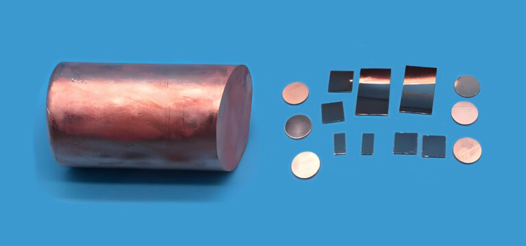
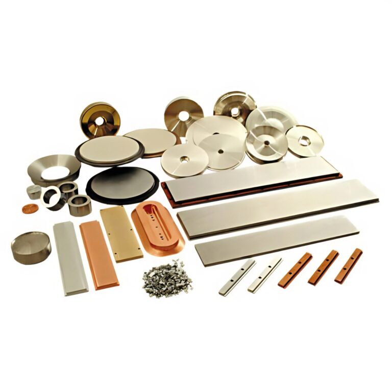
Tinsan Materials supplies single-crystal metal substrates for materials research, thin-film deposition, epitaxial growth, surface science, and related advanced applications.
Available materials include metal single crystals such as:
For Cu and Ni substrates, different crystallographic orientations, dimensions, thicknesses, purity requirements, and surface finishes can be discussed according to individual research requirements.
For graphene or 2D-material projects, customers are encouraged to provide information including the required material, orientation, dimensions, thickness, purity, surface finish, and intended application so that an appropriate substrate specification can be evaluated.
Conclusion
Single-crystal Cu(111) and Ni(111) substrates illustrate how strongly substrate engineering can influence graphene and 2D-material growth.
Cu(111) combines a graphene-compatible surface symmetry with very low carbon solubility, making it particularly attractive for monolayer graphene, domain alignment, large-area CVD growth, and transferable graphene films.
Ni(111) offers an even smaller lattice mismatch with graphene and stronger catalytic and interfacial interactions. Its higher carbon solubility introduces more complex segregation and precipitation behavior, but also makes Ni(111) exceptionally valuable for interface science, catalysis, multilayer growth studies, and hBN epitaxy.
Rather than asking simply whether Cu or Ni is the “better” substrate, researchers should consider what type of growth mechanism and interface they want to create.
As graphene and other 2D materials move from laboratory-scale crystals toward wafer-scale devices, the crystallographic orientation, purity, surface quality, and composition of the underlying metal substrate will become increasingly important variables in materials engineering.
References
1. Li, X. et al. Large-area synthesis of high-quality and uniform graphene films on copper foils. Science 324, 1312–1314 (2009). DOI: 10.1126/science.1171245.
2. Wu, T. et al. Fast growth of inch-sized single-crystalline graphene from a controlled single nucleus on Cu–Ni alloys. Nature Materials 15, 43–47 (2016).
3. Chen, T.-A. et al. Wafer-scale single-crystal hexagonal boron nitride monolayers on Cu(111). Nature 579, 219–223 (2020). DOI: 10.1038/s41586-020-2009-2.
4. Ma, K. Y. et al. Epitaxial single-crystal hexagonal boron nitride multilayers on Ni(111). Nature 606, 88–93 (2022). DOI: 10.1038/s41586-022-04745-7.
5. Shao, J. et al. Texture-engineered fabrication of ultraflat, 6-inch single-crystal Cu(111) wafers. Science Advances 11, eady1943 (2025). DOI: 10.1126/sciadv.ady1943.
6. Li, S. et al. Synthesis of single-crystal monolayer graphene on Cu/Ni(111) alloy foil. Nature Protocols (2026). DOI: 10.1038/s41596-026-01403-4.