-
 Single Crystals – Tinsan Materials")
- Ultra-High Thermal Conductivity: Up to 285 W/m·K, comparable to diamond.
- Wide Bandgap: ~6.2 eV, ideal for UV optoelectronic devices.
- High Electrical Resistivity: Excellent insulation properties.
- Superior Chemical and Thermal Stability: Suitable for harsh environments.
- Low Dielectric Constant and Loss: Enables high-frequency applications.
- High Mechanical Strength and Hardness: Durable under mechanical stress.
- Perfect Lattice Match for GaN: Supports high-quality epitaxial GaN growth.
-
 Single Crystals – Tinsan Materials")
- Direct Bandgap Semiconductor: Efficient absorption and emission of light; excellent for photovoltaic and photonic applications.
- High Optical Absorption: Especially in the visible spectrum.
- Strong Nonlinear Optical Effects: Useful for laser frequency conversion and optical modulation.
- Broad Transmission Range: From visible to near-infrared (0.7–3 μm).
- Low Defect Density: Ensures better carrier mobility and device performance.
- Good Chemical Stability: Under controlled conditions, suitable for device encapsulation.
- High Quantum Efficiency: Critical for optoelectronic device performance.
- High Dielectric Constant: Beneficial for high-frequency electronic applications.
-

- Wide Direct Bandgap: ~2.42 eV at room temperature, ideal for visible light applications.
- High Optical Transparency: Strong transmission from UV to visible spectral range.
- Excellent Epitaxial Compatibility: Ideal lattice matching with other II-VI semiconductor materials.
- Good Electrical Properties: Suitable for device applications in photodetection and photovoltaic fields.
- High Crystallinity: Available with low defect densities and precise orientation control.
-
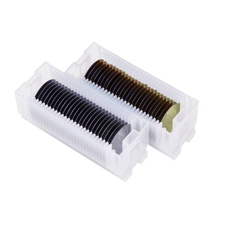

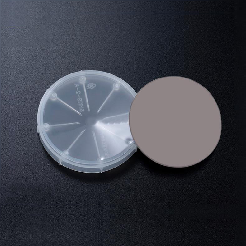
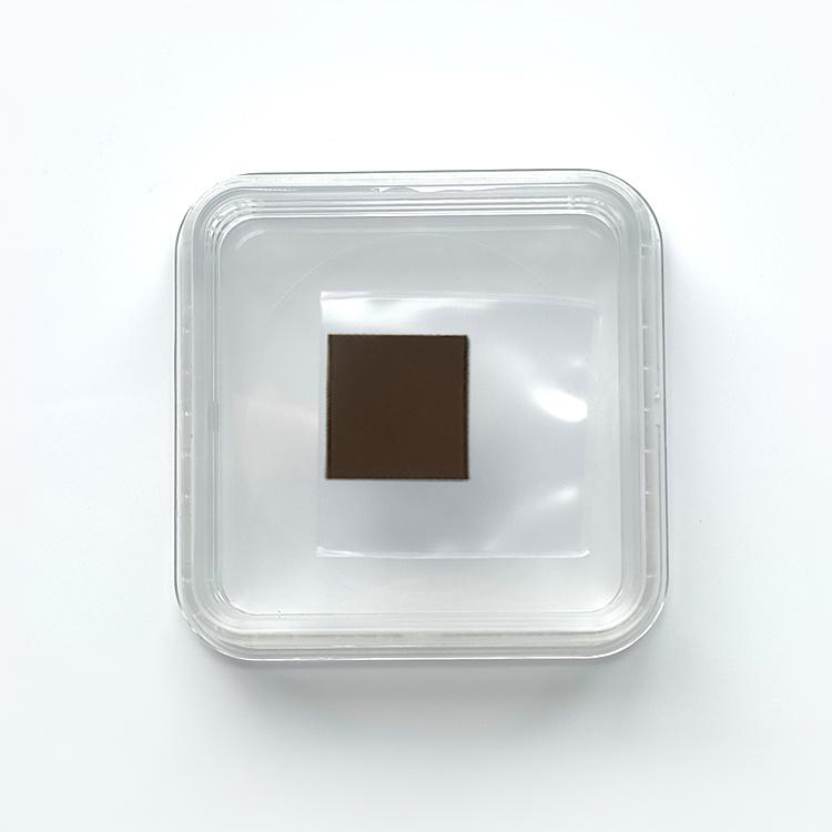
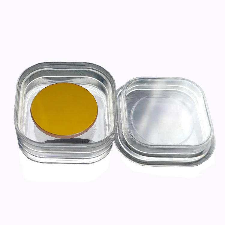
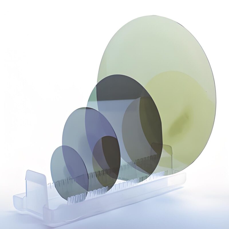
- Diameter Choices: 2″ to 12″ (or custom sizes).
- Doping Concentration: Custom doping profiles for N-type and P-type wafers.
- Thickness Variability: From ultra-thin wafers to thick substrates.
- Crystal Orientation: Standard orientations include <100>, <111>, <110>, with custom orientations available.
- Flat & Edge Treatment: Rounded, chamfered, or custom edge profiles.
- Surface Finishing:
- SSP (Single-Side Polished) or DSP (Double-Side Polished).
- Oxide coating, etched surfaces, or epitaxial layers upon request.
-

- Wide bandgap (3.2 eV for 4H-SiC)
- High thermal conductivity (~4.9 W/cm·K)
- Excellent chemical resistance
- High voltage breakdown strength
- Radiation hardness
- Suitable for GaN-on-SiC and epitaxial SiC device growth