Showing 13–24 of 34 results
-
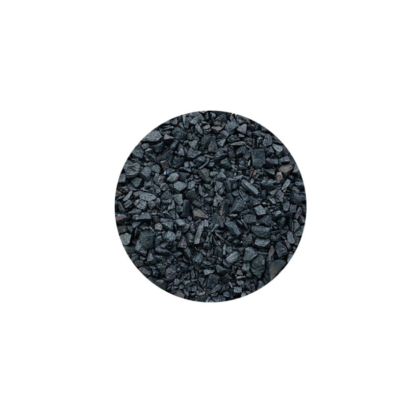
- Semiconducting Properties: CuSe is a p-type semiconductor material, making it useful in the development of electronic and optoelectronic devices.
- High Absorption Coefficient: It has a high absorption coefficient in certain wavelengths, making it suitable for photovoltaic and optical coating applications.
- Stability: Copper selenide is stable under a wide range of conditions, providing longevity for deposited thin films in various environmental settings.
- Excellent Conductivity: The material demonstrates good electrical conductivity, which is valuable in the context of solar energy harvesting and thermoelectric applications.
-
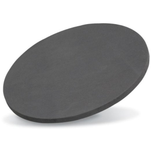
- High Purity: Ensures defect-free deposition for precision applications.
- Good Electrical Conductivity: Suitable for functional and conductive coatings.
- Stable Performance: Maintains chemical and thermal stability during sputtering processes.
- Customizable: Available in various dimensions and shapes for compatibility with sputtering systems.
-
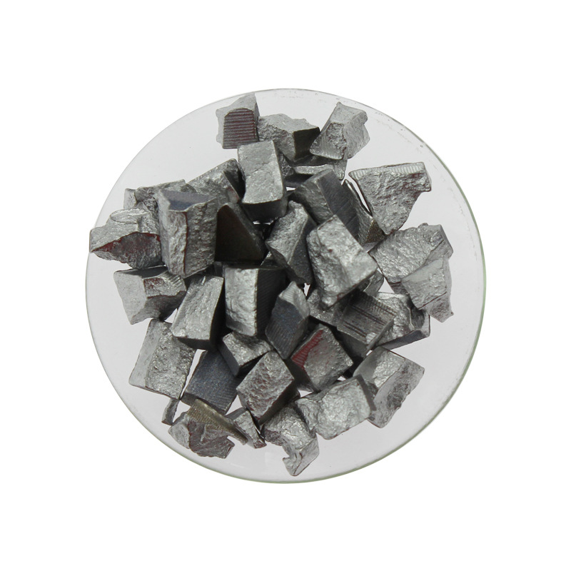
- Excellent IR Transparency: GeSe₂ has good transmission in the infrared spectrum, making it ideal for optical coatings and IR components.
- Semiconducting Properties: It exhibits semiconductor behavior, making it useful for electronics, photonics, and photovoltaic applications.
- Phase Change Behavior: GeSe₂ can undergo reversible phase changes, a property that is useful in memory storage devices.
- Good Film Uniformity: When evaporated, GeSe₂ forms uniform, high-quality thin films, suitable for precise optical coatings and electronic applications.
-
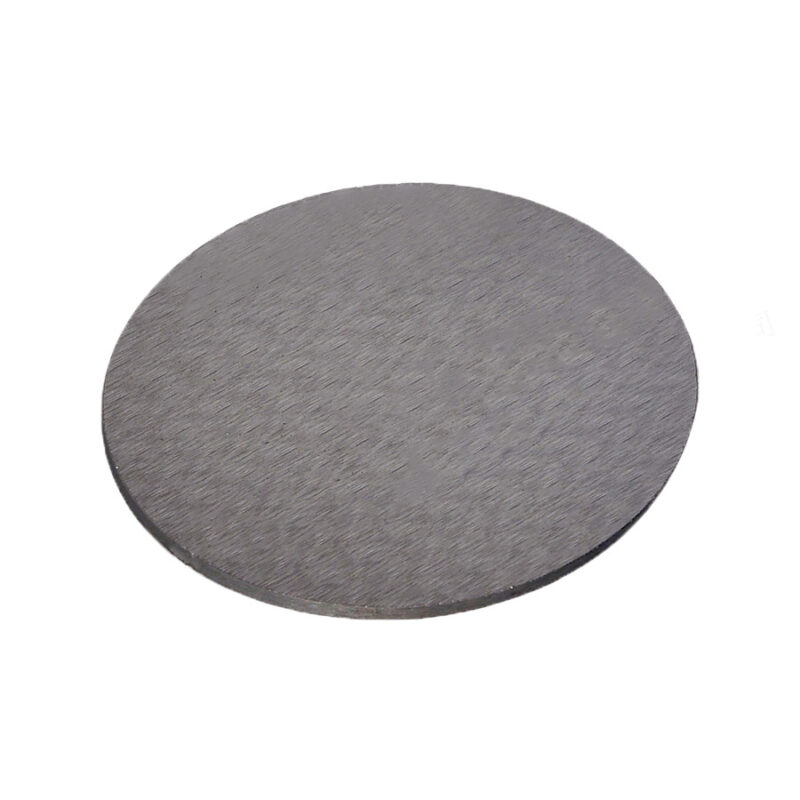
- Infrared Transparency: GeSe₂ offers excellent transmission in the infrared spectrum, making it suitable for IR optics and photonic applications.
- Phase-Change Properties: GeSe₂ is a key material in phase-change memory technology, providing the ability to switch between different states under thermal or electrical stimuli.
- Chemical and Thermal Stability: GeSe₂ thin films exhibit strong chemical resistance and can withstand high temperatures, ensuring longevity and performance in harsh conditions.
- High Refractive Index: GeSe₂ has a high refractive index, making it suitable for optical applications requiring materials with specific light-bending capabilities.
-
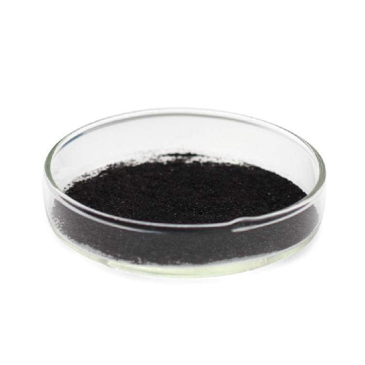
- High Purity: Ensures consistent performance for advanced applications.
- Semiconducting Properties: Ideal for electronic and optoelectronic devices.
- Wide Bandgap: Enables applications in high-performance photodetectors and solar cells.
- Thermal Stability: Supports use in high-temperature environments.
- Custom Particle Sizes: Available in nano and micron ranges.
- Versatile Applications: Spanning optoelectronics, photovoltaics, and research.
-
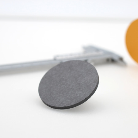
- High Optical Absorption: Ideal for solar energy harvesting applications.
- Semiconductor Versatility: Tunable electronic properties for various device designs.
- Eco-Friendly Composition: Cadmium-free material for safer and sustainable usage.
- Customizable Solutions: Specifications tailored to meet specific deposition requirements.
- High Purity: Ensures consistent and high-quality thin films.
-
$895.00
- High purity: 99.9% (3N) for consistent film composition
- Precise alloy ratio (1:1 at%) for uniform deposition
- Indium bonding + copper backing plate for efficient heat transfer
- Compatible with magnetron sputtering systems
- Supports stable deposition rates & low impurity levels
- Customizable sizes, thicknesses, and atomic ratios available
-
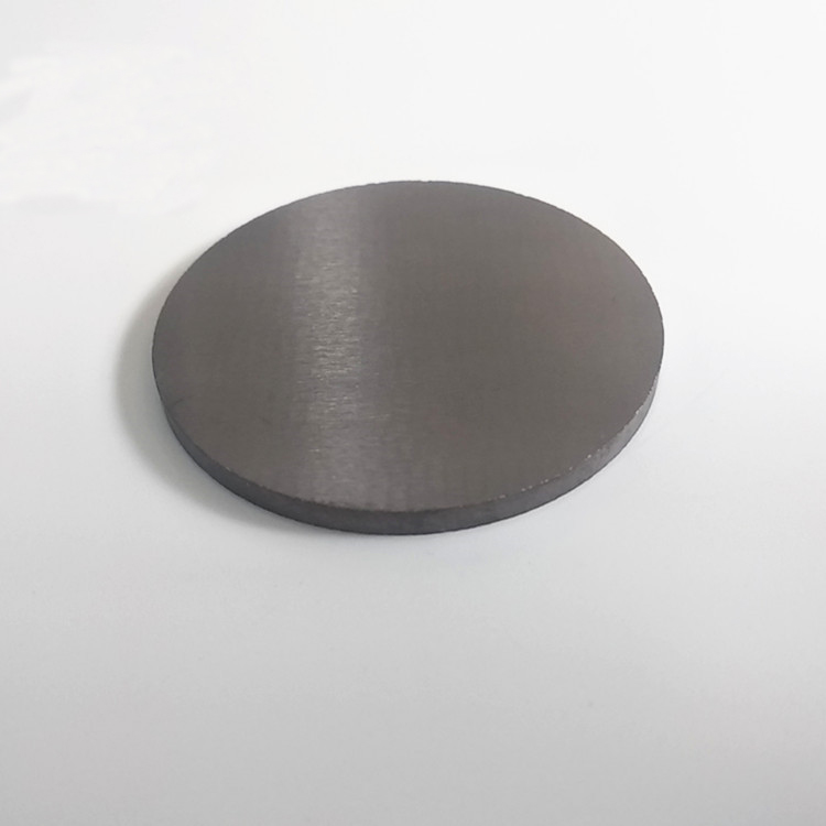
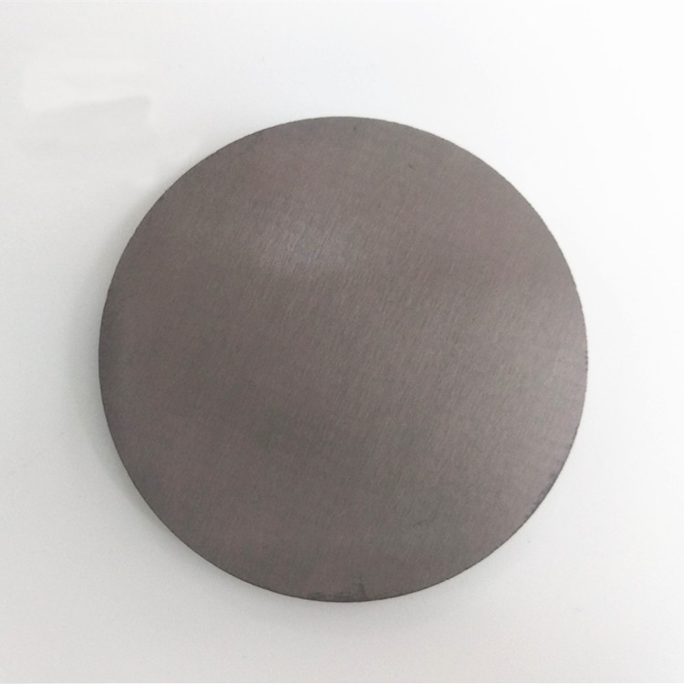
- High Purity: Ensures superior thin-film quality and device performance.
- Layered Structure: Facilitates easy exfoliation and 2D material synthesis.
- Stable Chemical Composition: Provides consistent results across various deposition processes.
- Excellent Optical and Electrical Properties: Ideal for advanced electronics and optoelectronics.
- Custom Configurations: Available in tailored sizes, shapes, and thicknesses for specific requirements.
-
- High Purity: ≥99.5% purity to ensure high-quality thin-film deposition.
- Unique Layered Structure: Facilitates superior electronic and optical properties for advanced applications.
- Superconducting Properties: Ideal for applications in superconducting electronics and quantum computing research.
- High Stability: Reliable performance under sputtering conditions with excellent chemical stability.
- Customizable: Tailored sizes and shapes for different deposition setups.
-
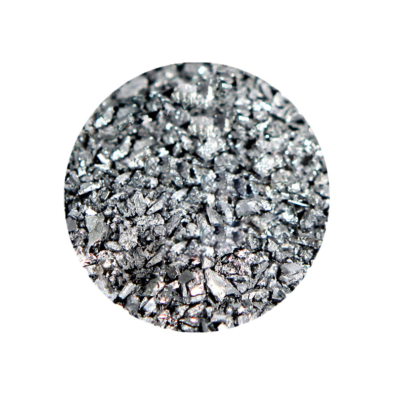
- High Absorption Coefficient: Sb2Se3 is known for its strong light absorption in the visible spectrum, making it ideal for thin-film solar cells.
- Stable Material: It exhibits good thermal and chemical stability, ensuring long-lasting performance in devices.
- Non-Toxic Alternative: Sb2Se3 is considered a safer and more environmentally friendly alternative to toxic materials like cadmium-based compounds in photovoltaic applications.
- Low Cost: It is a relatively cost-effective material for large-scale thin-film applications.
-
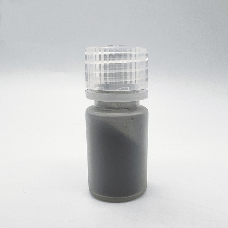
- High Absorption Coefficient: Ensures efficient light capture in photovoltaic applications.
- Direct Bandgap: Ideal for energy conversion and optoelectronics.
- Eco-Friendly Composition: A cadmium-free alternative for green energy solutions.
- Customizable Specifications: Tailored purity levels and particle sizes.
- Thermal Stability: Performs consistently under high-temperature conditions.
- Versatile Applications: Suitable for use in solar cells, thermoelectric devices, and optical coatings.
-
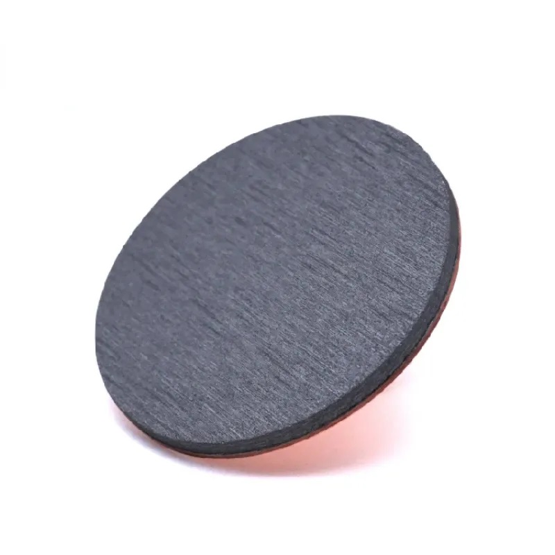
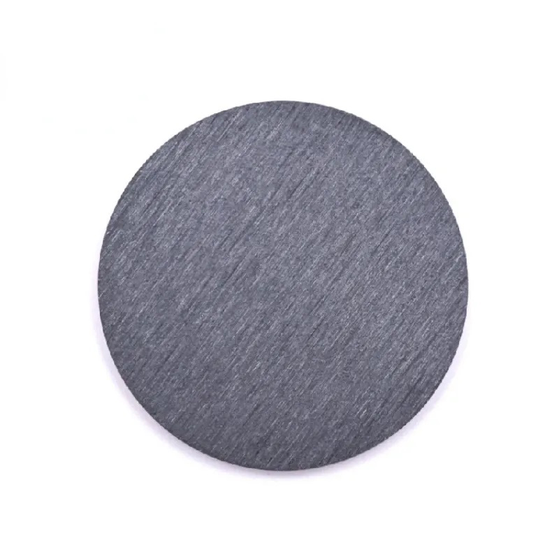
- High Absorption Coefficient: Sb₂Se₃ has a high absorption coefficient, which makes it effective for thin-film solar cells and light-harvesting applications.
- Bandgap: The material has a bandgap around 1.1 to 1.3 eV, ideal for photovoltaic devices aimed at capturing sunlight efficiently.
- Non-Toxic and Earth-Abundant: Sb₂Se₃ offers an environmentally friendlier and more sustainable alternative to other thin-film materials like cadmium-based compounds.
- Stable Crystal Structure: Sb₂Se₃ thin films exhibit a stable orthorhombic crystal structure, which contributes to their robustness in various electronic and energy-related applications.