Single Crystal Substrates - Tinsan Materials")
 Single Crystals - Tinsan Materials")
 Single Crystal Substrate - Tinsan Materials")


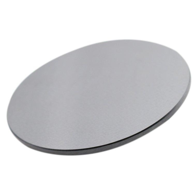
Cadmium Selenide (CdSe) Single Crystal Substrates
- Direct Bandgap Semiconductor: Efficient absorption and emission of light; excellent for photovoltaic and photonic applications.
- High Optical Absorption: Especially in the visible spectrum.
- Strong Nonlinear Optical Effects: Useful for laser frequency conversion and optical modulation.
- Broad Transmission Range: From visible to near-infrared (0.7–3 μm).
- Low Defect Density: Ensures better carrier mobility and device performance.
- Good Chemical Stability: Under controlled conditions, suitable for device encapsulation.
- High Quantum Efficiency: Critical for optoelectronic device performance.
- High Dielectric Constant: Beneficial for high-frequency electronic applications.
Custom products or bulk orders, please contact us for competitive pricing!
- Satisfaction Guaranteed
- No Hassle Refunds
- Secure Payments
Description
Cadmium Selenide (CdSe) single crystal substrates are widely used in optoelectronic applications, including infrared detectors, solar cells, light-emitting diodes (LEDs), and laser devices.
CdSe offers excellent direct bandgap semiconducting properties, high absorption efficiency in the visible spectrum, and strong nonlinear optical characteristics, making it ideal for high-performance electronic and photonic devices.
We supply high-purity, low-defect CdSe single crystal substrates tailored to meet the stringent requirements of both research institutions and industrial production.
Crystal Structure and Orientation:
- Chemical Formula: CdSe
- Crystal Structures:
- Wurtzite (Hexagonal) at room temperature
- Zinc Blende (Cubic) at higher temperatures
- Bandgap: ~1.74 eV (at 300K, direct bandgap)
- Lattice Constant (Hexagonal):
- a = 4.299 Å
- c = 7.010 Å
- Density: 5.81 g/cm³
- Melting Point: ~1268°C
- Available Orientations:
- (0001) C-plane (wurtzite structure)
- (111) for cubic structure
- Custom orientations upon request
Key Properties and Advantages:
- Direct Bandgap Semiconductor: Efficient absorption and emission of light; excellent for photovoltaic and photonic applications.
- High Optical Absorption: Especially in the visible spectrum.
- Strong Nonlinear Optical Effects: Useful for laser frequency conversion and optical modulation.
- Broad Transmission Range: From visible to near-infrared (0.7–3 μm).
- Low Defect Density: Ensures better carrier mobility and device performance.
- Good Chemical Stability: Under controlled conditions, suitable for device encapsulation.
- High Quantum Efficiency: Critical for optoelectronic device performance.
- High Dielectric Constant: Beneficial for high-frequency electronic applications.
Typical Applications:
- Infrared photodetectors and sensors
- Visible light and IR LEDs
- CdSe-based solar cells and tandem photovoltaic devices
- Electro-optic modulators
- Laser diodes and frequency conversion crystals
- Thin film deposition substrates for optoelectronic devices
- Research and development of quantum dots and nanostructures
- Terahertz devices and waveguides
Specifications:
| Diameter | 10 mm – 50 mm (customizable) |
| Thickness | 0.3 mm – 2.0 mm |
| Orientation | (0001), (111), or custom |
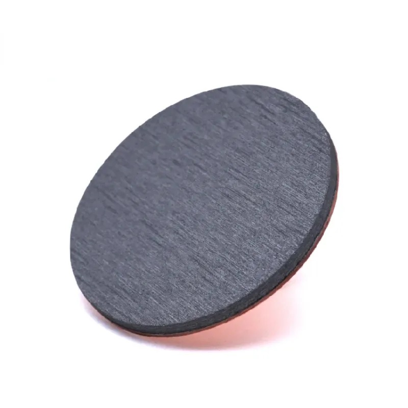
| Surface Finish | Single-side or double-side polished |
| Surface Quality | 20-10, 40-20, or 60-40 Scratch-Dig |
| Flatness | λ/10 at 632.8 nm |
| Parallelism | <10 arc seconds |
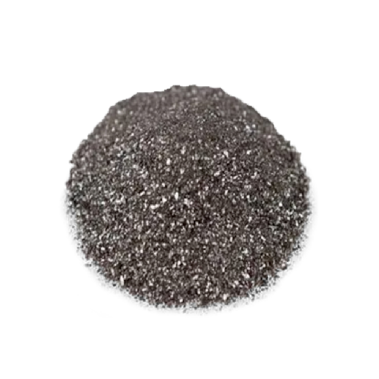
| Purity | ≥99.999% (5N) CdSe crystal |
| Coating Options | Protective coatings available upon request |
Available Sizes and Customization:
- Wafer Sizes: 10 mm, 20 mm, 25.4 mm (1 inch), 50.8 mm (2 inch), custom
- Thickness Options: 0.5 mm, 1 mm, 2 mm; other thicknesses available
- Polishing:
- SSP (Single-Side Polished)
- DSP (Double-Side Polished)
- Orientation Precision: ±0.5° or better
- Edge Treatments: Beveled, rounded, or customized edge shapes
- Surface Roughness: Down to atomic level (Ra < 3 Å) upon request
- Special Services:
- Laser scribing, custom shapes (squares, rectangles)
- Pre-coating services for thin film growth
Quality Assurance:
All CdSe substrates are subjected to rigorous quality control, including:
- High-resolution X-Ray Diffraction (HRXRD) analysis
- FTIR and UV-Vis-NIR spectrophotometry
- Surface roughness inspection with AFM
- Flatness and thickness verification by interferometry
- Visual inspection under microscope for pits, scratches, and inclusions
- Standard Class 1000 or Class 100 cleanroom packaging
Why Choose Our Cadmium Selenide (CdSe) Substrates?
- Premium-grade, defect-free CdSe single crystals
- Tailored sizes, orientations, and surface finishes
- Fast delivery with consistent quality assurance
- Expert consultation for custom device applications
- Extensive experience serving optoelectronics, laser, and R&D sectors
- Competitive pricing and reliable global logistics support
Ordering & Contact Information:
We offer flexible MOQ (Minimum Order Quantity) and competitive pricing. Our substrates are packaged in Class 100 cleanroom environments and shipped worldwide. For custom orders or technical inquiries, please contact us for a detailed consultation!
 Selenide Ceramic Sputtering Target High Pure 99.5%-99.9999% Customize – Tinsan Materials")