Single Crystal Substrates - Tinsan Materials")

Cadmium Sulfide (CdS) Single Crystal Substrates
- Wide Direct Bandgap: ~2.42 eV at room temperature, ideal for visible light applications.
- High Optical Transparency: Strong transmission from UV to visible spectral range.
- Excellent Epitaxial Compatibility: Ideal lattice matching with other II-VI semiconductor materials.
- Good Electrical Properties: Suitable for device applications in photodetection and photovoltaic fields.
- High Crystallinity: Available with low defect densities and precise orientation control.
Custom products or bulk orders, please contact us for competitive pricing!
- Satisfaction Guaranteed
- No Hassle Refunds
- Secure Payments
Description
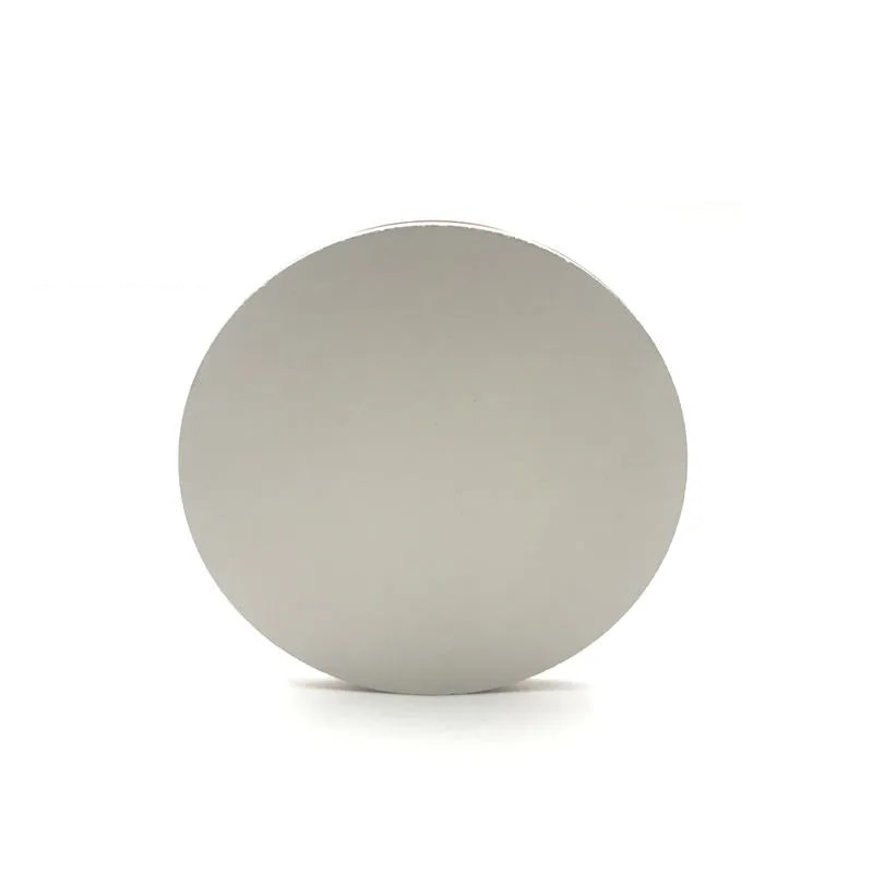
Cadmium Sulfide (CdS) single crystal substrates are wide bandgap II-VI semiconductor materials that exhibit excellent optical and electronic properties. CdS substrates are mainly used in optoelectronic devices, laser diodes, photodetectors, photovoltaic cells, and research into heterostructures and thin film epitaxy. With its direct bandgap (~2.42 eV at room temperature), CdS is particularly well-suited for visible light applications and acts as an important template material for the epitaxial growth of various II-VI compounds.
Key Features and Properties:
- Wide Direct Bandgap: ~2.42 eV at room temperature, ideal for visible light applications.
- High Optical Transparency: Strong transmission from UV to visible spectral range.
- Excellent Epitaxial Compatibility: Ideal lattice matching with other II-VI semiconductor materials.
- Good Electrical Properties: Suitable for device applications in photodetection and photovoltaic fields.
- High Crystallinity: Available with low defect densities and precise orientation control.
Typical Applications:
- Substrates for epitaxial growth of ZnCdS, CdTe, and other II-VI semiconductor films
- Solar cells and photovoltaic research
- Photodetectors and photosensors
- Laser diodes
- Electro-optical devices
- Piezoelectric devices
- Research into optoelectronic and photonic materials
Specifications:
| Material | Cadmium Sulfide (CdS) |
| Crystal Structure | Hexagonal (Wurtzite) or Cubic (Zinc Blende) |
| Chemical Formula | CdS |
| Lattice Constants | Hex: a = 4.136 Å, c = 6.714 Å; Cubic: a = 5.818 Å |
| Bandgap Energy | ~2.42 eV at 300 K |
| Transparency Range | 0.5 μm – 1.2 μm |
| Refractive Index | ~2.5 at 600 nm |
| Density | ~4.82 g/cm³ |
| Thermal Conductivity | ~0.15 W/cm·K |
| Melting Point | ~1750 °C |
| Typical Wafer Sizes | 10 mm, 20 mm, 25.4 mm |
| Thickness | 0.5 mm, 1.0 mm (customizable) |
| Orientation | (0001), (10-10), (11-20) or (100), (111) |
| Surface Finish | SSP or DSP |
| Defect Density | <5×10⁴ cm⁻² (typical) |
| Surface Roughness (RMS) | <1 nm after polishing (typical) |
| Growth Method | PVT or Bridgman Method |
Material Properties and Crystal Structure:
- Chemical Formula: CdS
- Crystal Structure: Hexagonal (Wurtzite) or Cubic (Zinc Blende) depending on growth conditions
- Growth Method: Physical Vapor Transport (PVT) or Bridgman method
- Lattice Constants:
- Hexagonal: a = 4.136 Å, c = 6.714 Å
- Cubic: a = 5.818 Å
Standard Product Sizes and Availability:
- Typical wafer diameters: 10 mm, 20 mm, 25.4 mm (1 inch)
- Thickness: 0.5 mm, 1.0 mm, or customized
- Orientation: (0001), (10-10), (11-20) for hexagonal; (100), (111) for cubic
- Surface Finish: Single-side polished (SSP) or double-side polished (DSP)
- Custom sizes, thicknesses, and orientations are available upon request
Customization Options:
- Custom crystallographic orientations
- Special thicknesses and sizes
- Surface treatments: chemical mechanical polishing (CMP) for ultra-flatness
- Wafer edge rounding or specific edge profiling
- Optional AR coatings for UV or visible spectrum
Packaging and Delivery:
- Packaged in Class 100 cleanroom environment
- Individually vacuum sealed in ESD-safe containers
- Protective packaging to prevent mechanical damage
Why Choose Our Cadmium Sulfide (CdS) Single Crystal Substrates?
- Strict quality control from crystal growth to final inspection
- High-purity materials ensuring excellent optical and electrical performance
- Flexible customization to meet your research or production needs
- Competitive pricing with fast lead times
- Comprehensive technical support from our experienced team
Ordering & Contact Information:
Tinsan Materials offers flexible MOQ (Minimum Order Quantity) and competitive pricing. Our substrates are packaged in Class 100 cleanroom environments and shipped worldwide. For custom orders or technical inquiries, please contact us for a detailed consultation!