Sputtering Target 99.9% Purity Ø50.8mm")
Manganese Selenide (MnSe) Sputtering Target | Mn:Se = 1:1 at% | 99.9% Purity | Ø50.8mm
$895.00
- High purity: 99.9% (3N) for consistent film composition
- Precise alloy ratio (1:1 at%) for uniform deposition
- Indium bonding + copper backing plate for efficient heat transfer
- Compatible with magnetron sputtering systems
- Supports stable deposition rates & low impurity levels
- Customizable sizes, thicknesses, and atomic ratios available
Custom products or bulk orders, please contact us for competitive pricing!
- Satisfaction Guaranteed
- No Hassle Refunds
- Secure Payments
Description
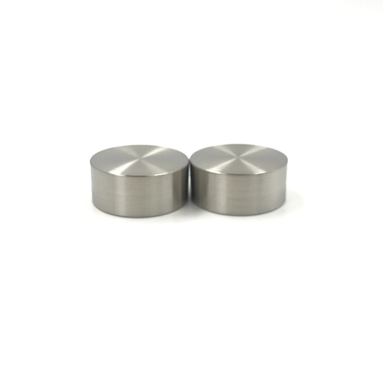
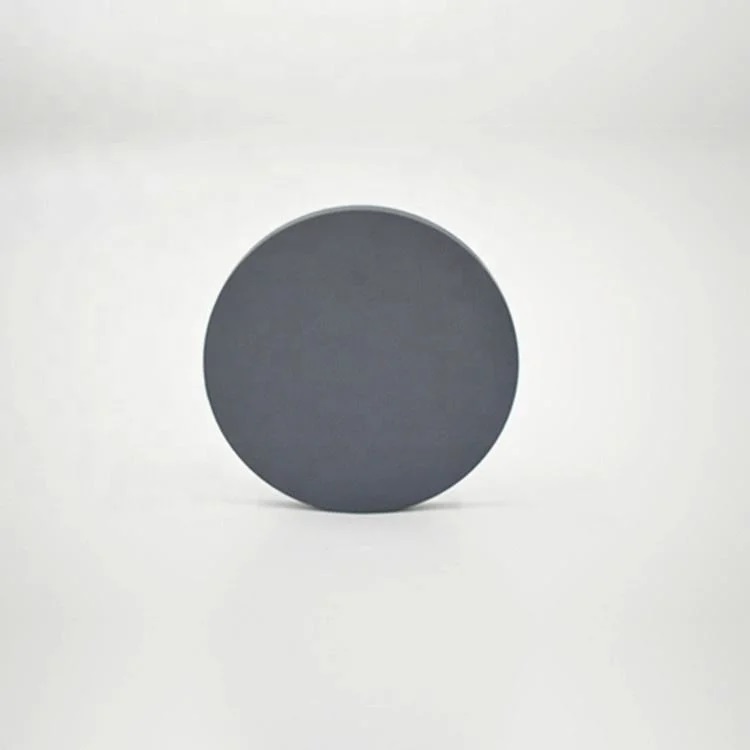
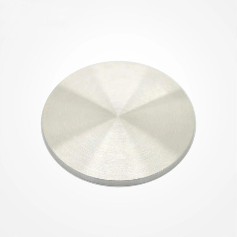
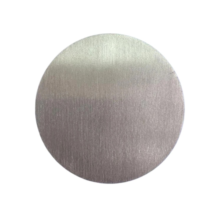
Our Manganese Selenide (MnSe) Sputtering Target is manufactured with a precise Mn:Se = 1:1 atomic ratio and 99.9% purity for high-performance thin film deposition. The target features a 50.8mm diameter, 3mm thickness, and is indium bonded to a 3mm copper backing plate with a magnetic clamp to support stable sputtering performance and improved heat dissipation.
This MnSe target is ideal for R&D laboratories, semiconductor process development, optical coatings, photovoltaic devices, and specialty electronic applications.
Technical Specifications
| Product Name | Manganese Selenide (MnSe) Sputtering Target |
| Chemical Ratio | Mn:Se = 1:1 at% |
| Purity | 99.9% (3N) |
| Diameter | 50.8mm (2 inch) or customized |
| Target Thickness | 3mm or customized |
| Backing Plate | 3mm Copper Backing Plate (Indium Bonded) |
| Mounting Option | Magnetic Base / Magnetic Pad |
| Form | Alloy Sputtering Target |
Key Features
- High purity: 99.9% (3N) for consistent film composition
- Precise alloy ratio (1:1 at%) for uniform deposition
- Indium bonding + copper backing plate for efficient heat transfer
- Compatible with magnetron sputtering systems
- Supports stable deposition rates & low impurity levels
- Customizable sizes, thicknesses, and atomic ratios available
Applications
- Semiconductor and microelectronic device fabrication
- R&D thin film deposition and experimental materials development
- IR optical coatings and photodetectors
- Surface engineering / protective coatings
- Photovoltaic energy materials & research
- Compound semiconductor technologies
Customization Options
| Purity | 99.9% – 99.995% |
| Diameter | 25.4mm / 50.8mm / 76.2mm / 101.6mm / Custom |
| Thickness | 2mm – 10mm or custom |
| Backing Plate | Cu / Mo / No backing plate |
| Bonding Method | Indium / Diffusion / Non-bonded |
- Custom specifications are available. Contact us for pricing based on size and purity requirements.
Ordering & Technical Support
Tinsan Materials provides flexible minimum order quantities, competitive pricing, and worldwide delivery. For custom specifications or technical inquiries, please feel free to contact us for a detailed consultation or email us at info@nbsvip.com.
Additional information
| Weight | N/A |
|---|---|
| Purity | 99.9% |
| Size | φ50.8mm x 3mm tk, bonded 3mm copper backing plate with magnetic pad attached |