 – Diameters 25.4 50 50.8 60 76.2 80 100 101.6 mm Custom Thickness & Size Options - Tinsan Materials")
 – Diameters 25.4 50.8 60 76.2 80 100 101.6 mm Custom Thickness & Size Options - Tinsan Materials")
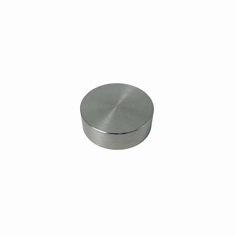
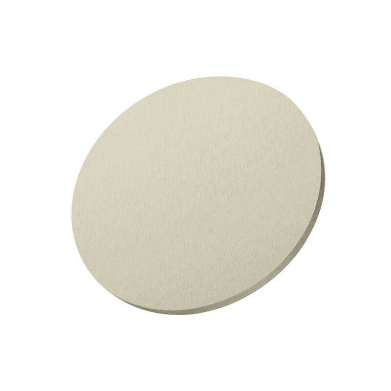
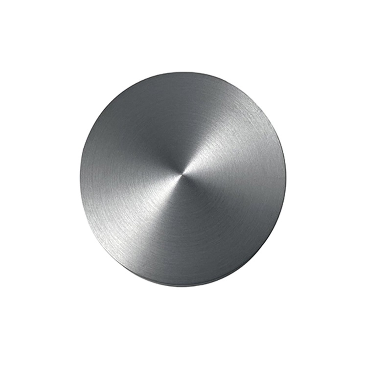
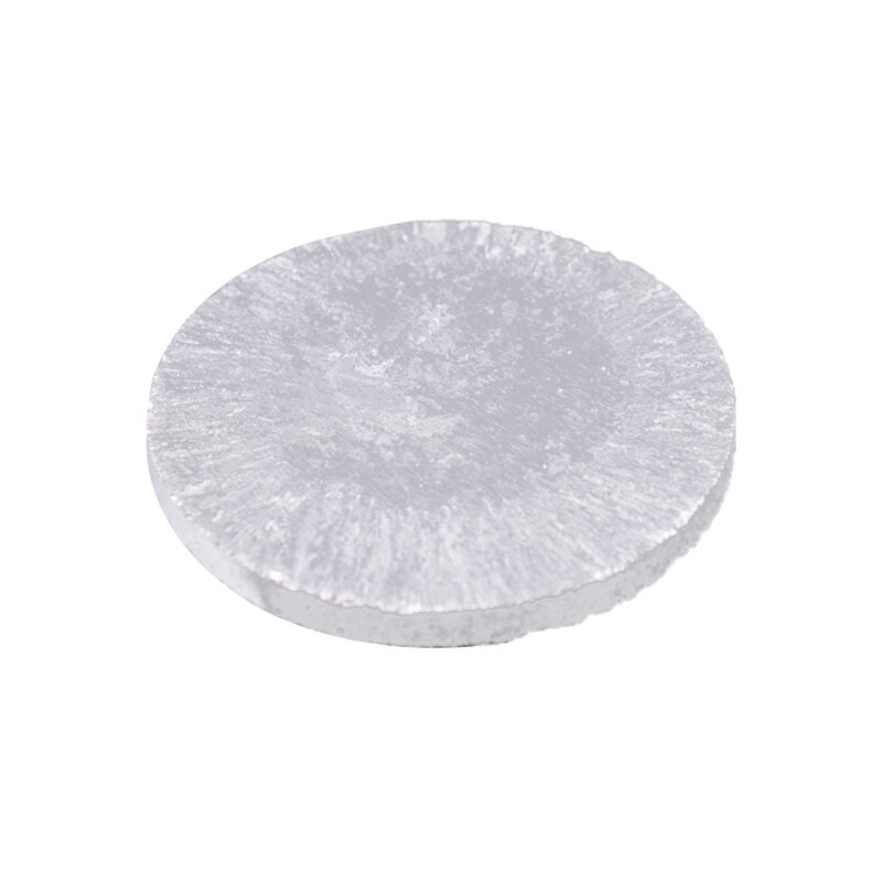
Silicon Sputtering Target P-Type 99.999% (5N) – Diameters 25.4 / 50 / 50.8 / 60 / 76.2 / 80 / 100 / 101.6 mm | Custom Thickness & Size Options
$46.00 – $200.00
- Ultra-high purity 5N Silicon ensures extremely low impurity levels and superior thin-film quality.
- Stable p-type electrical conductivity ideal for semiconductor and solar applications.
- Excellent sputtering uniformity with minimal particle generation.
- Multiple standard diameters in stock for fast order fulfillment.
- Fully customizable target dimensions, purity, and doping concentration.
Custom products or bulk orders, please contact us for competitive pricing!
- Satisfaction Guaranteed
- No Hassle Refunds
- Secure Payments
Description
Our 99.999% (5N) P-Type Silicon Sputtering Targets are manufactured for high-performance thin film deposition used in semiconductors, photovoltaic devices, microelectronics, and optical coatings.
We offer four standard diameters—25.4 mm, 50mm, 50.8 mm, 60mm, 76.2 mm, 80mm, 100mm, and 101.6 mm—with 3 mm, 4 mm, 5 mm, 6 mm, and 6.35mm thickness options (listed thicknesses will display corresponding prices).
Customized purity, diameter, doping concentration, thickness, and shapes are also available to meet specific R&D and production requirements.
Technical Specifications
| Product Name | P-Type Silicon Sputtering Target |
| Chemical Formula | Si |
| Purity | 99.999% (5N), custom options up to 6N |
| Conductivity Type | P-Type (Boron-doped as default; other dopants available) |
| Standard Diameters | 25.4 mm, 50 mm, 50.8 mm, 60 mm, 76.2 mm, 80 mm, 100 mm, 101.6 mm (custom diameter available) |
| Standard Thicknesses | 3 mm, 4 mm, 5 mm, 6 mm, 6.35 mm (custom thickness available) |
| Density | 2.33 g/cm³ |
| Shape Options | Round target (rectangular, square, and custom shapes available) |
| Packaging | Vacuum-sealed, anti-static, moisture-proof, and shock-protected |
Key Features
- Ultra-high purity 5N Silicon ensures extremely low impurity levels and superior thin-film quality.
- Stable p-type electrical conductivity ideal for semiconductor and solar applications.
- Excellent sputtering uniformity with minimal particle generation.
- Multiple standard diameters in stock for fast order fulfillment.
- Fully customizable target dimensions, purity, and doping concentration.
Applications
- Semiconductor device fabrication (p-type layers)
- Thin-film deposition for ICs and microelectronics
- Solar cell manufacturing (P-type silicon layers)
- Optical coatings and dielectric layers
- MEMS and sensor development
- R&D laboratories and university research
Customization Options
We provide tailored silicon sputtering targets according to customer requirements:
- Purity Customization:
- 4N (99.99%)
- 4N5 (99.995%)
- 5N (99.999%)
- 6N (99.9999%)
- Diameter Customization
- Standard: 25.4 / 50 / 50.8 / 60 / 76.2 / 80 / 100 / 101.6 mm
- Available custom diameters: 10–300 mm
- Thickness Customization
- Standard: 3 / 4 / 5 / 6 / 6.35 mm
- Custom thickness available upon request
- Doping Customization
- Boron (B) – standard p-type dopant
- Aluminum (Al), Gallium (Ga), Indium (In) available on request
- Tunable resistivity and dopant concentration
- Shape & Bonding Options
- Round, rectangular, square, or special shapes
- Bonding to backing plates (Mo, Cu, SS) for high-power sputtering systems
Ordering & Technical Support
We provide flexible minimum order quantities, competitive pricing, and worldwide delivery. For custom specifications or technical inquiries, please feel free to contact us for a detailed consultation or email us at info@nbsvip.com.
Additional information
| Weight | N/A |
|---|---|
| PURITY | 99.999% (P-Type) |
| DIAMETER | 25.4mm, 50mm, 50.8mm, 60mm, 76.2mm, 80mm, 100mm, 101.6mm |
| THICKNESS | 3mm, 4mm, 5mm, 6mm, 6.35mm |


 ZnO Single Crystal Substrate , 10×10×0.5 mm, Single-Side Polished (O-Face Polished)