- Tinsan Materials")
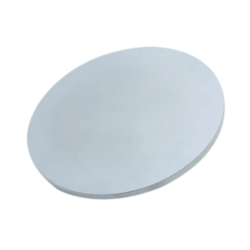
ZnO Single Crystal Substrate <0001>, 10×10×0.5 mm, Single-Side Polished (O-Face Polished)
$335.00
- Crystal Orientation: <0001>
- High Purity & Low Defect Density ensuring stable epitaxial growth
- Single-Side Polished (SSP / 1sp) with high-quality O-face polished surface
- Precise Dimensions: 10 mm × 10 mm × 0.5 mm
- High Surface Quality: Low roughness suitable for MBE, PLD, sputtering, and CVD
- Excellent Physical Properties: High transparency in UV, robust thermal stability
- Ideal for Research & Industrial Applications
Custom products or bulk orders, please contact us for competitive pricing!
- Satisfaction Guaranteed
- No Hassle Refunds
- Secure Payments
Description
Zinc Oxide (ZnO) Single Crystal Substrate with crystallographic orientation <0001> and dimensions 10 × 10 × 0.5 mm is precisely manufactured for advanced optoelectronic and semiconductor research. This substrate is single-side polished (SSP / 1sp) with the O-face polished, ensuring excellent surface flatness and low defect density for epitaxial growth, thin-film deposition, and device fabrication.
ZnO single crystals offer direct wide bandgap (3.37 eV), high exciton binding energy (60 meV), and excellent thermal and chemical stability, making them ideal for UV optoelectronics, piezoelectric devices and transparent electronics.
Key Features
- Crystal Orientation: <0001>
- High Purity & Low Defect Density ensuring stable epitaxial growth
- Single-Side Polished (SSP / 1sp) with high-quality O-face polished surface
- Precise Dimensions: 10 mm × 10 mm × 0.5 mm
- High Surface Quality: Low roughness suitable for MBE, PLD, sputtering, and CVD
- Excellent Physical Properties: High transparency in UV, robust thermal stability
- Ideal for Research & Industrial Applications
Technical Specifications
| Material | ZnO (Zinc Oxide) Single Crystal |
| Crystal Orientation | <0001>, custom orientation available |
| Size | 10 mm x 10 mm x 0.5 mm, custom size available |
| Polishing | O-face polished (SSP), custom polish available |
| Crystal Structure | Wurtzite (Hexagonal) |
| Space Group | P6₃mc |
| Lattice Constants | a = 3.252 Å, c = 5.313 Å |
| Density | 5.7 g/cm³ |
| Thermal Conductivity | 0.6-1.2 W/cm·K |
| Thermal Expansion | αₐ = 4.75×10⁻⁶ K⁻¹, α𝑐 = 2.9×10⁻⁶ K⁻¹ |
| Hardness (Mohs) | ~4.5 |
| Orientation Accuracy | ±0.5° |
| Applications | GaN/AlN epitaxy, SAW/BAW devices, UV detectors, piezoelectric sensors |
Applications
- UV LEDs & UV Lasers
- Piezoelectric & Acoustic Devices
- Transparent Electronics
- Thin-Film Deposition (MBE/PLD/CVD/Sputtering)
- Optoelectronic Research
- Semiconductor Devices
- Sensor Development
Customization Options
Tinsan Materials offers custom ZnO substrates with:
- Orientation: <0001>, <10-10>, <11-20>, etc.
- Dimensions: wafers, squares, custom shapes
- Thickness: 0.2 mm – 1 mm or customized
- Polishing: SSP / DSP / O-face / Zn-face
- Surface roughness levels
- Special cleaning or coating treatments
Ordering & Technical Support
Tinsan Materials provides flexible minimum order quantities, competitive pricing, and worldwide delivery. For custom specifications or technical inquiries, please feel free to contact us for a detailed consultation or email us at info@nbsvip.com.
Additional information
| Weight | 0.1 kg |
|---|