Showing 469–480 of 686 results
-

- High Thermoelectric Efficiency: Sb₂Te₃ exhibits excellent thermoelectric performance with a high figure of merit (ZT) near room temperature, making it one of the most effective materials for energy conversion and cooling applications.
- Phase-Change Properties: Its ability to rapidly switch between different phases with thermal cycling makes Sb₂Te₃ ideal for memory devices such as phase-change random-access memory (PCRAM).
- Topological Insulator Properties: Sb₂Te₃ is used in cutting-edge research into topological insulators, with potential applications in quantum computing and advanced electronics.
- Customizable Thin Films: Sputtering targets allow for controlled deposition of Sb₂Te₃ films with tailored thickness, composition, and properties for specific device requirements.
-
 Crystals – Tinsan Materials")
- Exceptional Photorefractive Effect: Superior for dynamic holography and real-time optical data storage.
- High Electro-optic Coefficient: Enabling efficient light modulation.
- Low Optical Damage Threshold: Excellent for high-sensitivity photorefractive applications.
- Piezoelectric and Pyroelectric Properties: Supporting applications in sensors and transducers.
- Nonlinear Optical Response: Suitable for second harmonic generation (SHG) and other nonlinear optical processes.
- Broad Transmission Range: Transparent from visible to near-infrared wavelengths.
-
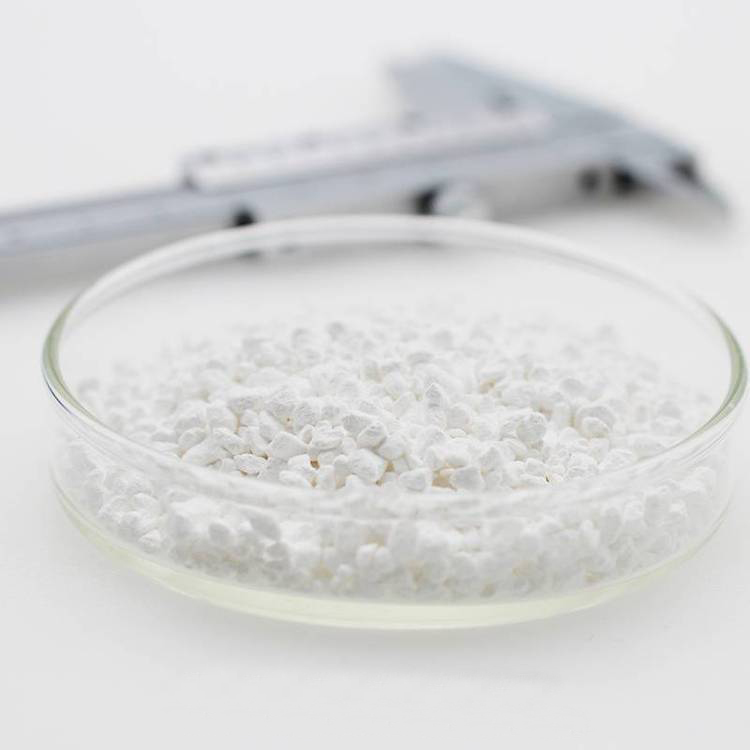
- High Strength-to-Weight Ratio: Scandium foil offers excellent mechanical strength relative to its weight, making it a lightweight yet durable material ideal for aerospace and military applications.
- High Melting Point: Scandium has a high melting point of 1,540°C (2,804°F), providing exceptional performance in high-temperature environments.
- Corrosion Resistance: Scandium foil exhibits remarkable resistance to corrosion, especially in acidic and saline environments, making it suitable for challenging environmental conditions.
- Thermal Stability: The material maintains its mechanical properties even at elevated temperatures, ensuring long-term reliability in high-heat applications.
- Non-toxic and Biocompatible: Scandium foil is non-toxic, making it safe for medical and other applications where human exposure may occur. Its biocompatibility is also an asset for certain implantable medical devices.
- Electrical Conductivity: Although not as conductive as copper, scandium foil still offers good electrical conductivity, making it suitable for various electronic applications.
- Lightweight: Scandium is a relatively light metal, which helps reduce the weight of components and systems, particularly in aerospace and defense applications.
-
- High Purity: Scandium pellets are typically offered at purities of 99.9% or higher, ensuring the creation of defect-free thin films.
- Improved Strength: Scandium’s addition to thin films or alloys significantly improves strength and durability, making it valuable in high-stress environments such as aerospace.
- Optical and Electronic Properties: Scandium offers unique optical and electronic properties, making it suitable for specialized coatings and electronic components.
- Versatility in Deposition: Scandium can be used in various deposition methods, including thermal and e-beam evaporation, to create thin films for high-performance applications.
-
- Strength-to-Weight Ratio: Scandium significantly improves the strength-to-weight ratio of aluminum alloys, making it essential for lightweight, high-performance materials used in aerospace and other industries.
- Corrosion Resistance: Scandium helps improve the corrosion resistance of aluminum alloys, making them more durable and long-lasting, especially in harsh environments.
- Thermal Stability: Scandium alloyed with aluminum offers excellent thermal stability, making it suitable for high-temperature applications.
- Electrical Conductivity: Scandium enhances the conductivity of materials, making it a key component in electronics and energy storage systems like fuel cells.
-

Scandium sputtering targets are essential in applications that require lightweight, high-performance coatings, particularly in the semiconductor, aerospace, and advanced materials sectors. Despite its rarity, scandium’s unique properties make it a valuable material for cutting-edge technologies.
-
- High Purity: Ensures superior performance in sensitive applications.
- Thermal Stability: Maintains stability at high temperatures.
- Exceptional Optical Properties: High transparency in the UV and IR spectra.
- Low Thermal Expansion: Ideal for use in advanced ceramics.
- Customizable Particle Sizes: Nano and micrometer scales available.
- Excellent Chemical Resistance: Resists degradation in harsh environments.
-

- High Dielectric Constant: Sc₂O₃ is known for its high dielectric constant, making it useful in capacitors and semiconductor devices.
- Thermal Stability: Sc₂O₃ maintains its properties even at elevated temperatures, making it suitable for harsh environments.
- Optical Transparency: Sc₂O₃ is transparent across a wide range of wavelengths, from UV to IR, which is beneficial in optical coatings and devices.
- Corrosion Resistance: Sc₂O₃ thin films are highly resistant to chemical corrosion, enhancing the longevity of coated surfaces.
-
- Ultra-high purity (≥99.9%).
- Superior thermal and chemical stability.
- Precise dimensions for uniform deposition.
- Customizable sizes and shapes available.
- Wide application in advanced technology industries.
-
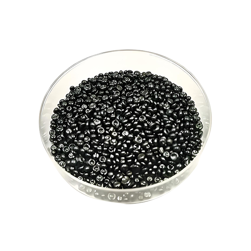

- Photoconductive Properties: Selenium changes its electrical conductivity when exposed to light, making it essential for optoelectronic devices such as photodetectors and xerography.
- Semiconductor Capabilities: Selenium is a key element in semiconductor applications, offering high photoelectric sensitivity and versatility in electronic components.
- High Purity: Selenium evaporation materials are typically offered in high-purity levels (≥ 99.9%) for optimal thin-film deposition and consistent results.
- Compatibility with PVD Techniques: Selenium pellets can be easily evaporated using thermal or electron-beam evaporation, providing stable and uniform thin films.
- Infrared Optics: Selenium-based compounds, like cadmium selenide (CdSe), are used in infrared detectors and imaging technologies due to their IR transparency.
-

- Purity: High-purity selenium (typically 99.9% or higher) ensures the quality of the deposited films and consistent performance.
- Photoconductivity: Selenium is highly photoconductive, making it ideal for optoelectronic and photovoltaic applications.
- Customizable Size and Shape: Selenium sputtering targets are available in different forms, including discs, plates, and custom shapes, to fit a variety of PVD systems.
- Thermal and Electrical Properties: Selenium films offer excellent thermal and electrical properties, crucial for semiconductor and photovoltaic devices.
-

$10.00 – $335.00
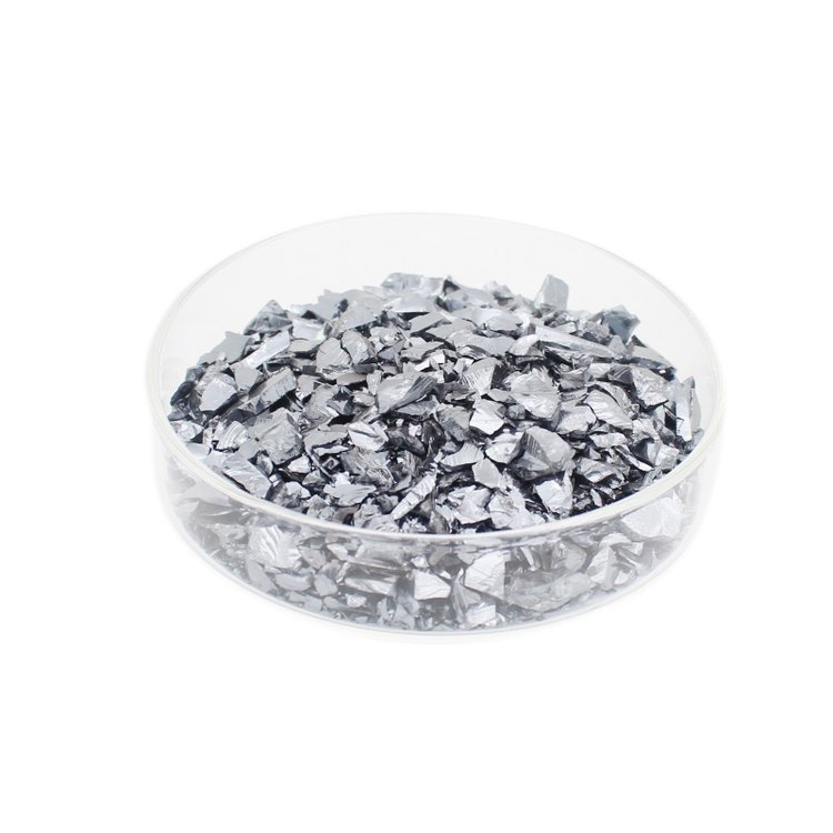
- High Purity: Silicon pellets typically have a purity of ≥ 99.9%, ensuring high-quality thin-film deposition with minimal contamination.
- Semiconductor Properties: Silicon’s intrinsic semiconducting properties make it crucial for electronic and optoelectronic applications.
- Thermal Stability: Silicon can withstand high temperatures during deposition, providing stable and uniform films.
- Infrared Transparency: Silicon exhibits excellent transparency in the infrared (IR) range, making it suitable for IR optics and coatings.
- Easy Evaporation: Silicon pellets are easily evaporated using thermal or electron-beam evaporation techniques, allowing for precise control in thin-film deposition.