Single Crystal Substrates - Tinsan Materials")

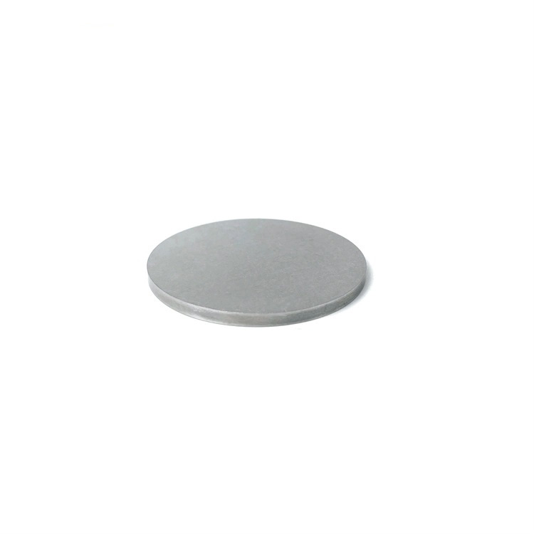
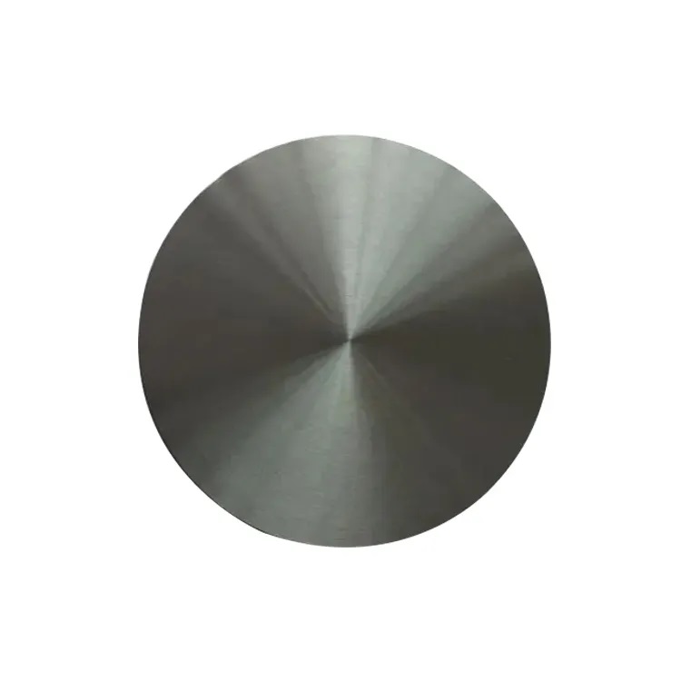
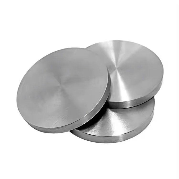
Potassium Tantalate (KTaO3) Single Crystal Substrates
- High Structural Perfection: Ideal lattice matching for growing oxide thin films such as superconductors and ferroelectric films.
- Excellent Dielectric Properties: High dielectric constant makes it suitable for tunable capacitors and microwave applications.
- Low Optical Absorption: Transparent in the visible to near-infrared spectrum, useful for optoelectronic devices.
- High Mechanical and Chemical Stability: Ensures robustness in diverse environments.
- Ferroelectric and Quantum Paraelectric Behavior: Suitable for research in quantum phase transitions and low-temperature physics.
- Epitaxial Growth Substrate: Preferred for epitaxy of functional oxide materials such as high-temperature superconductors, ferroelectric, and multiferroic materials.
Custom products or bulk orders, please contact us for competitive pricing!
- Satisfaction Guaranteed
- No Hassle Refunds
- Secure Payments
Description
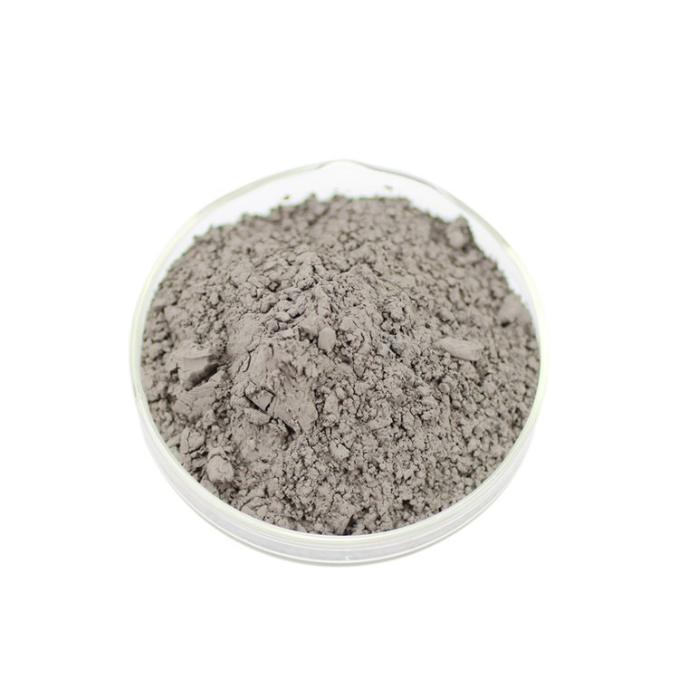
Potassium Tantalate (KTaO₃) is a high-quality, cubic perovskite-type oxide single crystal known for its excellent dielectric, ferroelectric, and electro-optic properties.
KTaO₃ substrates are widely used in research and device fabrication involving next-generation electronics, quantum materials, tunable microwave devices, and epitaxial film growth.
We provide premium-grade KTaO₃ substrates with high structural perfection, precise orientation, and exceptional surface quality to meet the stringent requirements of advanced applications.
Crystal Structure and Orientation:
- Chemical Formula: KTaO₃
- Crystal Structure: Cubic perovskite
- Space Group: Pm3m
- Lattice Constant: a = 3.989 Å
- Density: ~8.01 g/cm³
- Melting Point: ~1650°C
- Dielectric Constant: ~5000 at low temperatures; ~200 at room temperature
- Bandgap: ~3.6 eV (direct bandgap)
- Available Orientations:
- <100> (most commonly used)
- <110> and <111> orientations are available upon request
Key Properties and Advantages:
- High Structural Perfection: Ideal lattice matching for growing oxide thin films such as superconductors and ferroelectric films.
- Excellent Dielectric Properties: High dielectric constant makes it suitable for tunable capacitors and microwave applications.
- Low Optical Absorption: Transparent in the visible to near-infrared spectrum, useful for optoelectronic devices.
- High Mechanical and Chemical Stability: Ensures robustness in diverse environments.
- Ferroelectric and Quantum Paraelectric Behavior: Suitable for research in quantum phase transitions and low-temperature physics.
- Epitaxial Growth Substrate: Preferred for epitaxy of functional oxide materials such as high-temperature superconductors, ferroelectric, and multiferroic materials.
Typical Applications:
- Epitaxial growth of perovskite oxides (e.g., SrTiO₃, BaTiO₃, and cuprate superconductors)
- Tunable microwave devices and resonators
- Quantum materials research (quantum paraelectrics, superconductivity)
- High-k dielectric thin films
- Electro-optical and optoelectronic devices
- Photonic and nonlinear optical components
- Sensors and actuators
- Low-temperature quantum physics experiments
Specifications:
| Crystal Type | KTaO₃ Single Crystal |
| Orientation | <100>, <111>, <110> |
| Standard Sizes | 10 × 10 mm², 20 × 20 mm², 2″ wafers (customizable) |
| Thickness | 0.5 mm, 1 mm, 2 mm (customizable) |
| Surface Finish | Double-Side Polished (DSP) |
| Surface Quality | 10-5 or 20-10 Scratch-Dig (MIL-PRF-13830B) |
| Surface Flatness | λ/10 @ 632.8 nm |
| Parallelism | < 10 arc seconds |
| Orientation Accuracy | ±0.5° |
| Defect Density | Very Low (Epi-Ready quality available) |
Available Sizes and Customization:
- Standard Substrate Sizes:
- 10 × 10 mm²
- 15 × 15 mm²
- 20 × 20 mm²
- 1 inch, 2 inches diameter
- Custom Sizes:
- Custom shapes and thicknesses available on request
- Thickness Options:
- 0.5 mm, 1.0 mm, 2.0 mm standard, others customizable
- Surface Options:
- Double-Side Polished (DSP) for epitaxial applications
- Custom one-side polished (OSP) on request
- Edge Options:
- Laser cut, beveled, or rounded edges for safety
Quality Assurance:
Our KTaO₃ substrates undergo rigorous inspection to guarantee premium quality:
- X-ray Diffraction (XRD) analysis to ensure crystal orientation and purity
- Atomic Force Microscopy (AFM) for surface roughness control (<0.5 nm RMS available)
- Optical Microscopy inspection for surface defect minimization
- Surface flatness measured by Interferometry
- Cleanroom packaging in Class 1000 environment
Why Choose Our Potassium Tantalate Single Crystal Substrates?
- High crystalline quality with low defect density
- Excellent dielectric and quantum properties for advanced research
- Epi-ready surface preparation
- Wide range of customization options in size, thickness, and orientation
- Fast lead times and global shipping
- Technical support and after-sales assistance available
Ordering & Contact Information:
Tinsan Materials offers flexible MOQ (Minimum Order Quantity) and competitive pricing. Our substrates are packaged in Class 100 cleanroom environments and shipped worldwide. For custom orders or technical inquiries, please contact us for a detailed consultation!