Showing 61–72 of 696 results
-
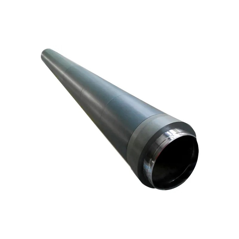
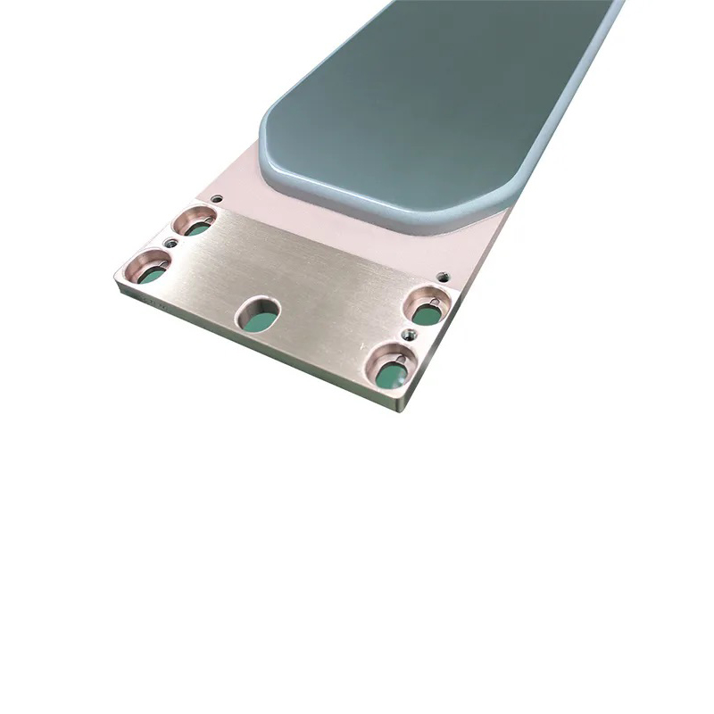
- High Optical Transparency: AZO offers excellent transparency in the visible spectrum, making it ideal for applications requiring clear conductive films.
- Good Electrical Conductivity: Despite its transparency, AZO provides high electrical conductivity, which is critical in photovoltaic cells and touchscreens.
- Environmentally Friendly: Unlike ITO, AZO does not rely on scarce or expensive elements like indium, making it a more sustainable and cost-effective choice.
- Thermal and Chemical Stability: AZO films maintain stability under various temperature and environmental conditions, making them suitable for outdoor and industrial applications.
- Low Reflectivity: AZO films are known for their low reflectance, which is beneficial in display technologies to reduce glare and improve visibility.
-
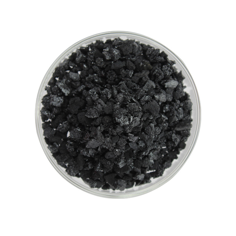
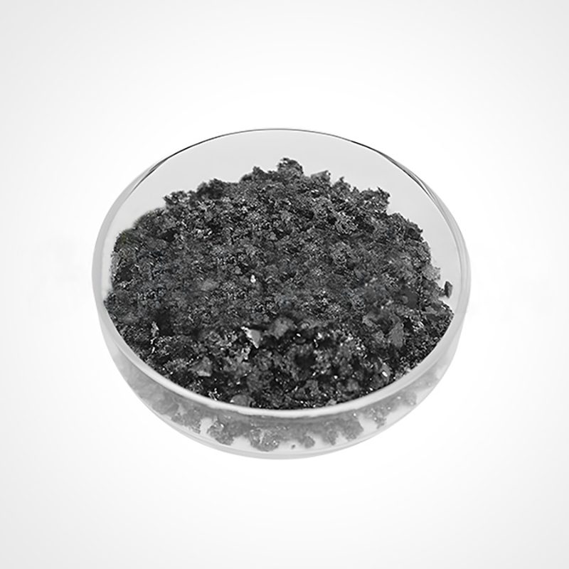
- High Hardness: Boron is extremely hard, making it ideal for applications requiring wear resistance.
- High Melting Point: Boron has a high melting point of 2,075°C, making it suitable for high-temperature deposition processes.
- Excellent Chemical Resistance: Boron is chemically inert in many environments, offering durability in corrosive conditions.
- Neutron Absorption: Boron is capable of absorbing neutrons, making it useful in nuclear shielding applications.
- Low Density: Boron is lightweight, making it suitable for applications requiring minimal mass, such as aerospace and optics.
-
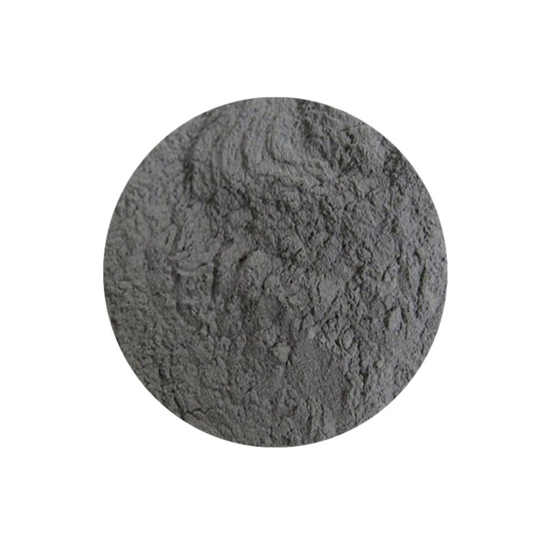
- High Melting Point: Boron has a melting point of 2,076°C, making it suitable for high-temperature applications.
- Low Density: It is lightweight compared to many metals, which makes it advantageous for use in lightweight materials and alloys.
- Hardness: Boron is extremely hard and is a key component in creating super-hard materials like boron carbide.
- Neutron Absorption: Boron’s ability to absorb neutrons without forming long-lived radioactive isotopes makes it vital for radiation shielding and nuclear control rods.
- High Thermal Conductivity: It efficiently conducts heat, which is beneficial for thermal management in electronics and other high-temperature systems.
-
Boron (B) sputtering targets are high-purity materials used in physical vapor deposition (PVD) processes, particularly sputtering, to deposit thin films of boron onto various substrates. These targets are widely used in industries such as electronics, optics, and materials science due to boron’s unique properties.
-
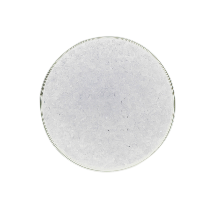
- High Purity: Ensures optimal performance in sensitive applications.
- Thermal Stability: Maintains integrity under high-temperature conditions.
- Optical Transparency: Ideal for optical and electronic coatings.
- Versatile Uses: Applicable across industries including electronics, optics, and materials science.
- Customizable Sizes: Available in various pellet sizes to meet specific requirements.
-
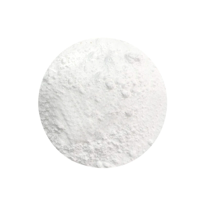
- High Purity: Available with ≥99.9% purity for consistent performance.
- Excellent Glass-Forming Properties: A key ingredient in borosilicate glass and optical fibers.
- Thermal Stability: Withstands high temperatures without decomposition.
- Chemical Inertness: Resistant to most chemicals, making it ideal for specialized applications.
- Customizable Particle Sizes: Nano (<100 nm) and micro (1–50 µm) options available or customized.
- Eco-Friendly: Non-toxic and compliant with environmental standards.
-
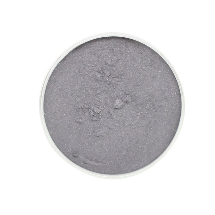
- Extreme Hardness: Mohs hardness of 9.5, second only to diamond and cubic boron nitride.
- Low Density: Lightweight material ideal for aerospace and defense applications.
- High Thermal Stability: Exceptional performance at high temperatures.
- Chemical Inertness: Resistant to most acids and alkalis.
- Superior Wear Resistance: Ideal for abrasive and protective applications.
- Customizable Particle Sizes: Nano (<100 nm) and micro (1–50 µm) grades available or customized.
-
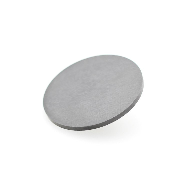
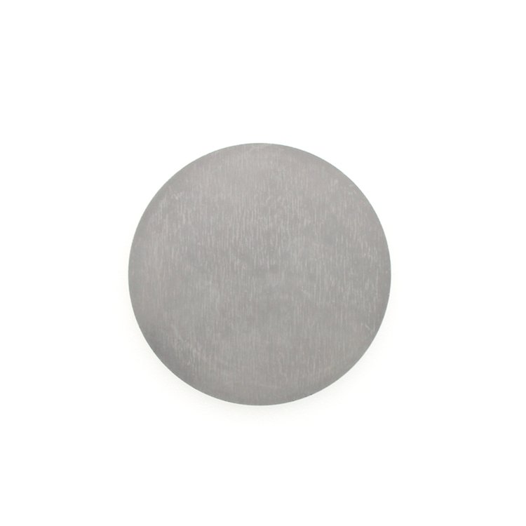
- Exceptional Hardness: High resistance to wear and abrasion.
- Chemical Stability: Resistant to acids and alkalis, ensuring longevity in extreme environments.
- Lightweight: Facilitates applications where low weight is critical.
- High Purity: Delivers superior film quality and consistency.
-
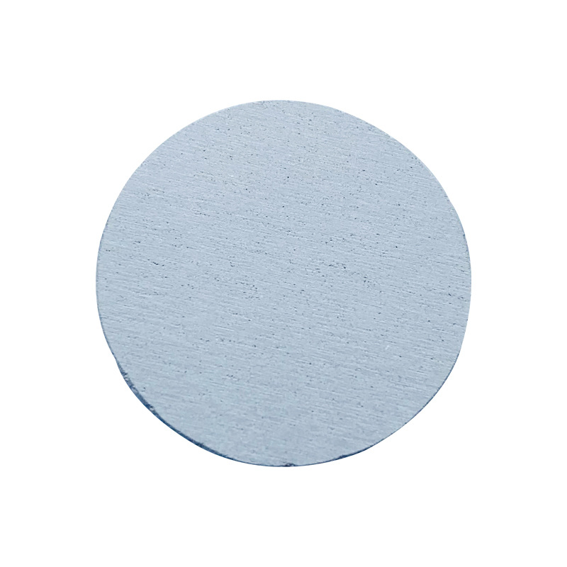
Barium (Ba) sputtering targets are high-purity materials used in physical vapor deposition (PVD) processes, particularly sputtering, to create thin films on various substrates. Barium targets are typically used in the production of optical coatings, semiconductor devices, and other advanced materials due to their unique properties.
-

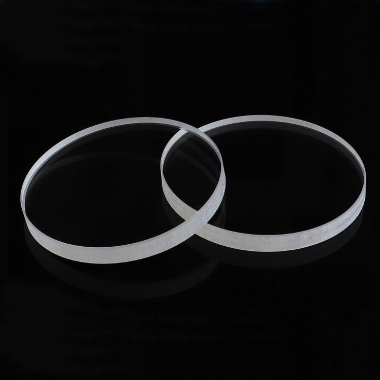
- Ultra-Wide Transmission Range (DUV to IR): 150 nm to 12–15 μm.
- Low Refractive Index: Minimizes reflection losses without extensive coatings.
- High Radiation Resistance: Suitable for high-radiation environments such as space and nuclear detectors.
- Low Dispersion: Excellent for optical systems requiring minimal chromatic aberration.
- Good Mechanical Properties: Higher fracture toughness compared to other fluoride crystals.
- Low Absorption and High Optical Quality: Especially critical in high-resolution spectroscopic systems.
- Compatibility with High-Energy Lasers: Due to high laser-induced damage threshold.
- Ease of Cleaving and Processing: Supports cost-effective manufacturing.
- Stable Physical and Chemical Properties: Good moisture resistance compared to other fluorides.
-
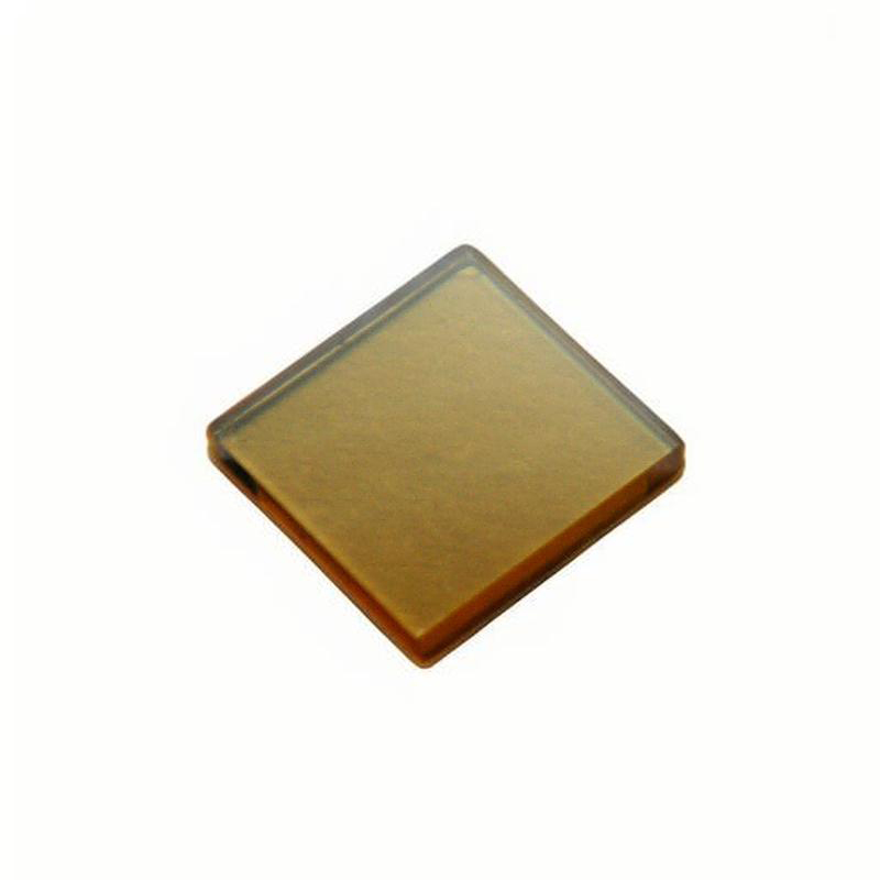
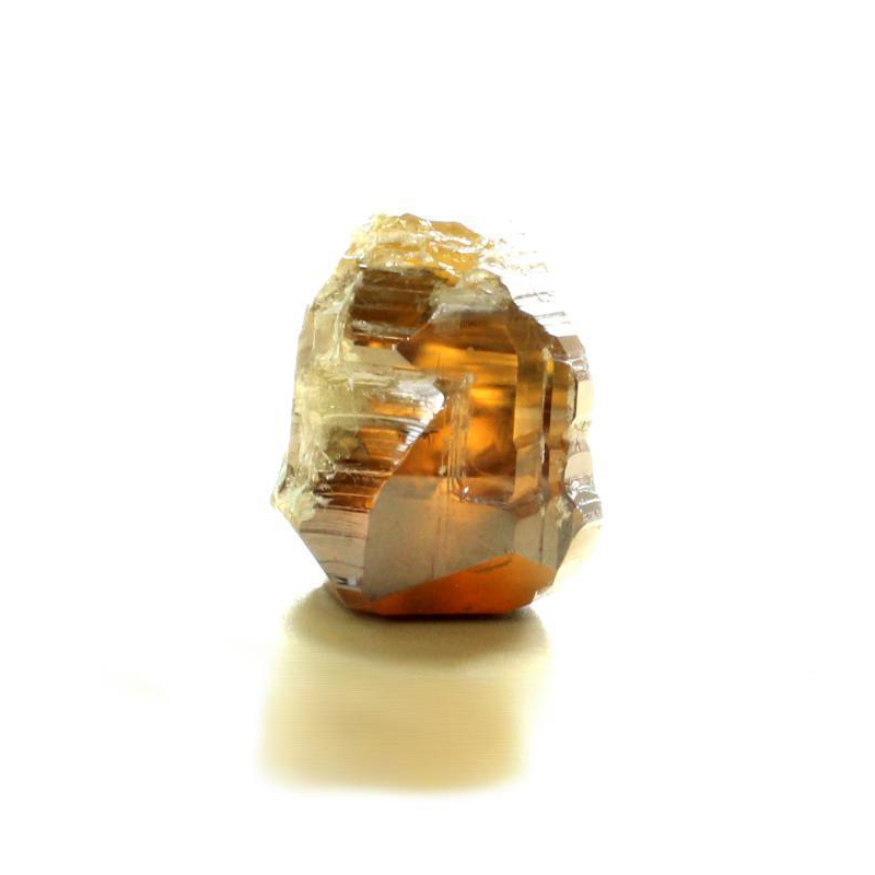
- Ferroelectric behavior with spontaneous polarization
- Extremely high dielectric constant (up to thousands near Curie temperature)
- Piezoelectric and electro-optic effects
- Cubic structure at high temperature, tetragonal below Curie temperature (~120°C)
- Suitable for integration with other perovskite materials
- Atomically smooth surfaces achievable for epitaxy
-
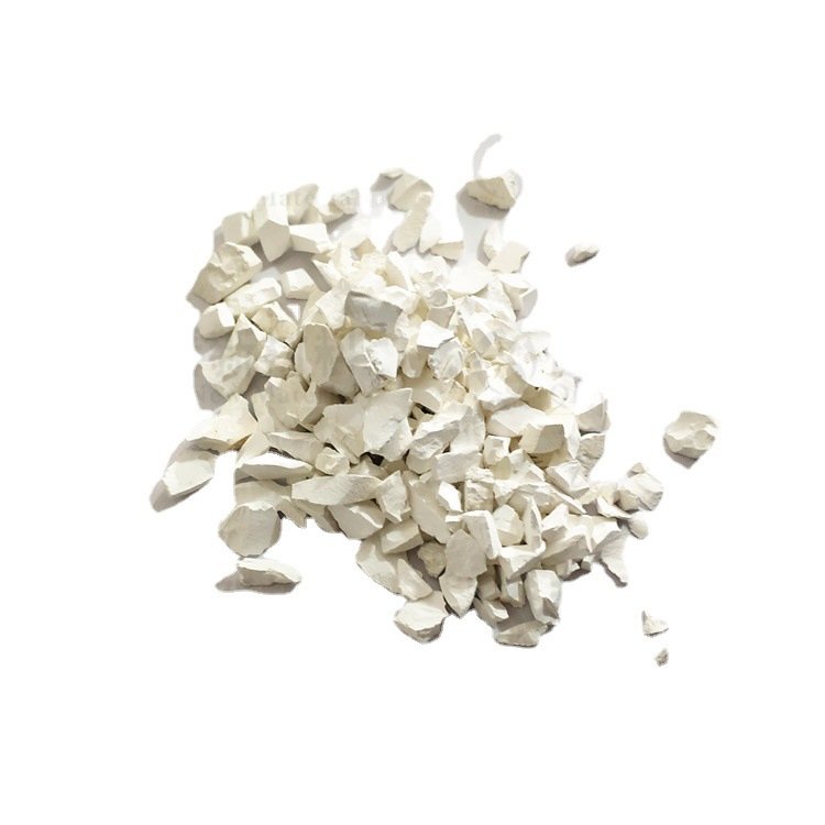
- High purity (≥99.99%).
- Outstanding dielectric and ferroelectric properties.
- Suitable for thin-film deposition techniques such as PVD.
- Uniform pellet size for consistent results in industrial and research settings.
- Custom sizes and packaging available.