Showing 97–108 of 171 results
-

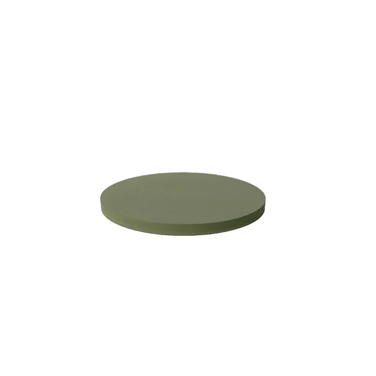
- Semiconducting Properties: NiO is a p-type semiconductor with excellent electrical characteristics, making it suitable for use in electronic devices and energy storage systems.
- Optical Transparency: NiO films exhibit optical transparency in the visible range, making them ideal for use in transparent conductive films and display technologies.
- High Thermal Stability: NiO sputtering targets offer good thermal stability, allowing them to withstand high-temperature processing in various applications.
- Corrosion Resistance: NiO films provide excellent corrosion resistance, making them useful for protective coatings in chemically aggressive environments.
- Catalytic Activity: NiO has good catalytic properties, which are utilized in sensors and catalytic applications for gas detection and environmental monitoring.
-
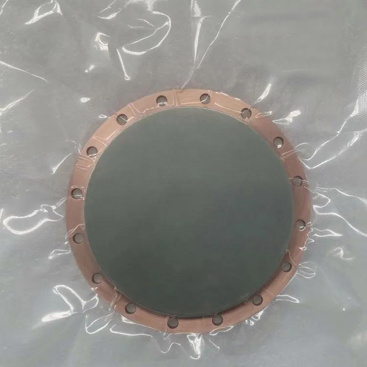
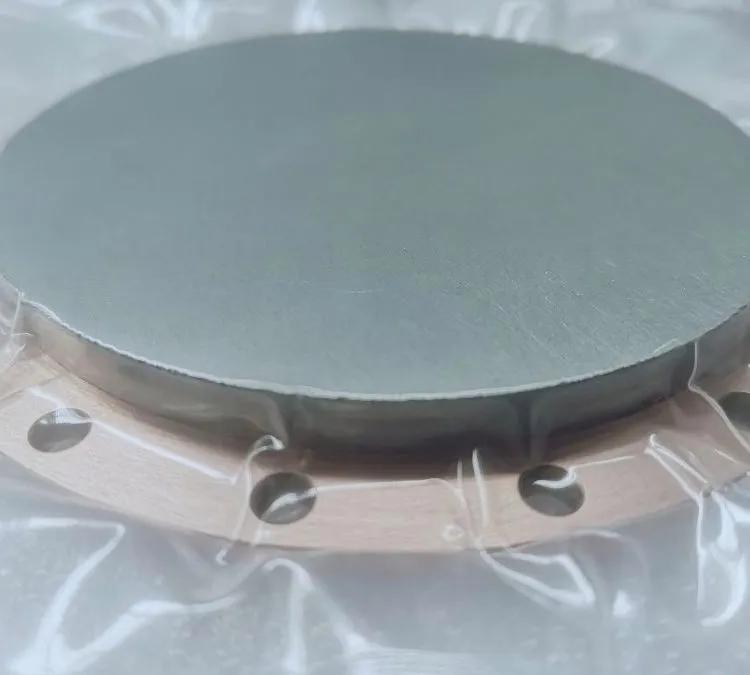
- High Purity: Up to 99.99% for superior film quality.
- Customizable Dimensions: Available in various sizes and shapes to fit specific equipment.
- Excellent Performance: Delivers consistent and uniform thin films.
- Thermoelectric and IR Applications: Suitable for deposition in advanced electronics and sensor systems.
-
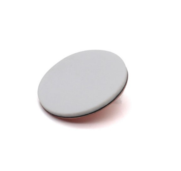
- Chemical Resistance: PTFE is highly resistant to a wide range of chemicals, including acids, bases, and solvents, making it ideal for corrosive applications.
- Non-Stick Surface: The material’s low surface energy allows for the production of coatings that resist adhesion, which is beneficial in various applications.
- Electrical Insulation: Excellent dielectric properties make it a great choice for insulating electrical components.
- High Temperature Resistance: PTFE can withstand a broad temperature range, maintaining its performance even at high temperatures.
- Durable Coatings: PTFE sputtering targets produce uniform and durable coatings with low friction and high wear resistance.
-
- High Piezoelectric Coefficient: Enables efficient conversion of mechanical energy to electrical energy and vice versa.
- Stable Dielectric Properties: Ensures reliable performance in high-frequency applications.
- Customizable Compositions: Tailored Zr/Ti ratios to meet specific functional requirements.
- High Purity and Uniformity: Ensures consistent film deposition with minimal defects.
- Versatile Deposition: Compatible with RF and DC magnetron sputtering systems.
-
- High Purity: Available in high-purity grades to ensure the production of defect-free thin films, which are essential for optical and electronic applications.
- Flame Retardant Properties: When deposited as a thin film, Sb₂O₃ enhances the flame retardant capabilities of various materials, particularly polymers and textiles.
- Optical Transparency: Sb₂O₃ has excellent transparency in the UV and visible light spectrum, making it a suitable material for optical applications.
- Thermal Stability: Its stability at high temperatures makes it useful in processes where thermal resistance is necessary.
-
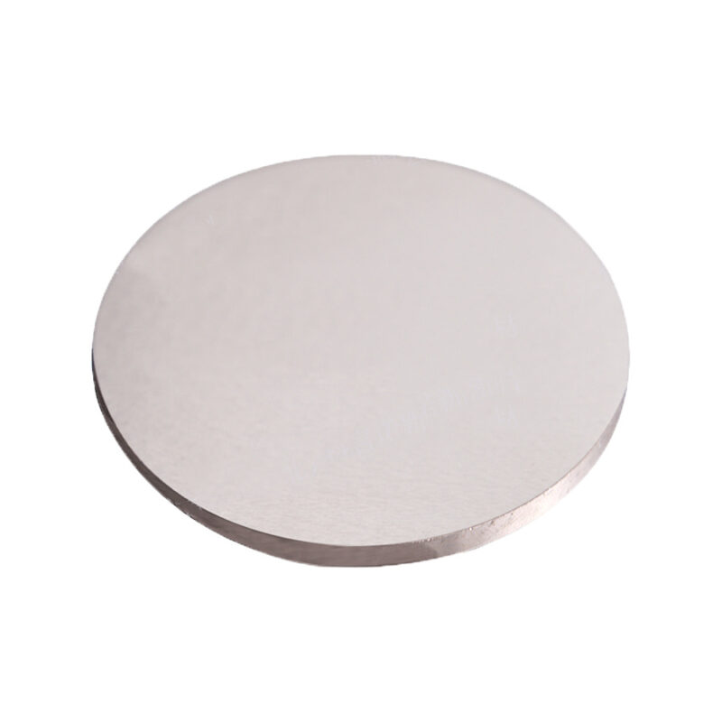
- High Optical Absorption: Sb₂S₃ is known for its strong absorption in the visible and near-infrared regions, making it ideal for photovoltaic and optoelectronic applications.
- Environmentally Friendly: Sb₂S₃ is composed of elements that are abundant and less toxic compared to other heavy metals used in similar applications.
- Tunability: The bandgap of Sb₂S₃ can be tuned by modifying deposition parameters, allowing for control over its optical and electronic properties in thin films.
- Thermoelectric Properties: Sb₂S₃ is being explored for its potential to generate electrical energy from thermal gradients, offering promise in energy-harvesting devices.
-
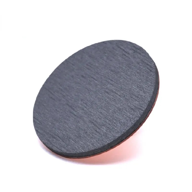
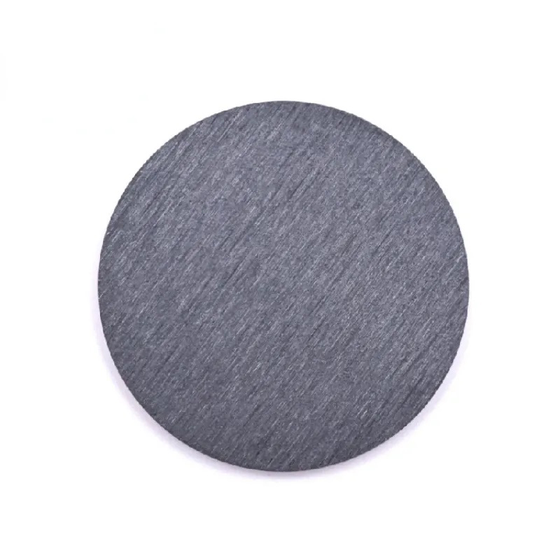
- High Absorption Coefficient: Sb₂Se₃ has a high absorption coefficient, which makes it effective for thin-film solar cells and light-harvesting applications.
- Bandgap: The material has a bandgap around 1.1 to 1.3 eV, ideal for photovoltaic devices aimed at capturing sunlight efficiently.
- Non-Toxic and Earth-Abundant: Sb₂Se₃ offers an environmentally friendlier and more sustainable alternative to other thin-film materials like cadmium-based compounds.
- Stable Crystal Structure: Sb₂Se₃ thin films exhibit a stable orthorhombic crystal structure, which contributes to their robustness in various electronic and energy-related applications.
-
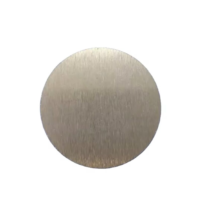

- High Thermoelectric Efficiency: Sb₂Te₃ exhibits excellent thermoelectric performance with a high figure of merit (ZT) near room temperature, making it one of the most effective materials for energy conversion and cooling applications.
- Phase-Change Properties: Its ability to rapidly switch between different phases with thermal cycling makes Sb₂Te₃ ideal for memory devices such as phase-change random-access memory (PCRAM).
- Topological Insulator Properties: Sb₂Te₃ is used in cutting-edge research into topological insulators, with potential applications in quantum computing and advanced electronics.
- Customizable Thin Films: Sputtering targets allow for controlled deposition of Sb₂Te₃ films with tailored thickness, composition, and properties for specific device requirements.
-
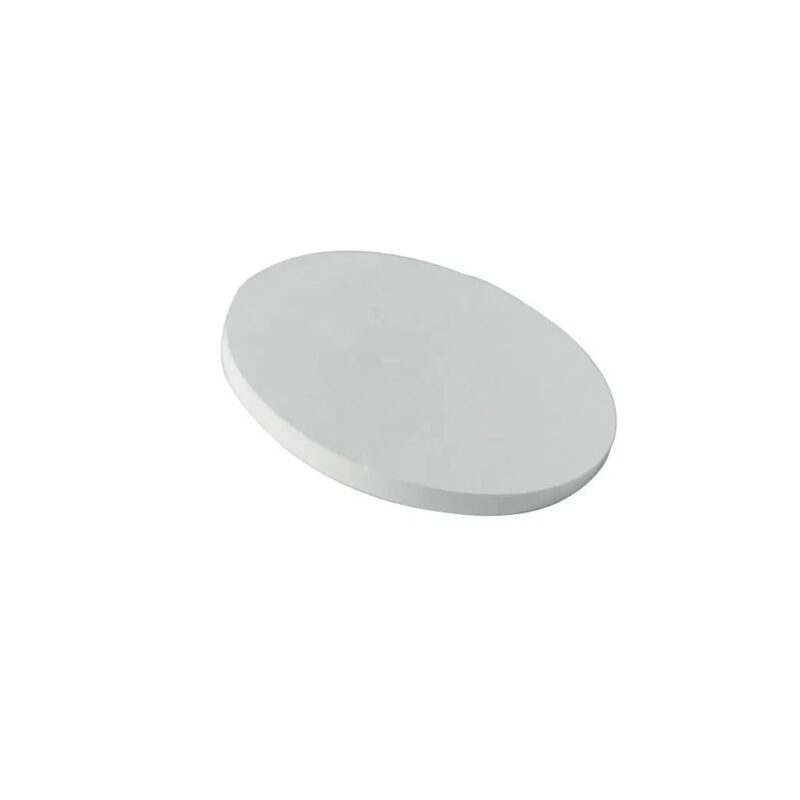
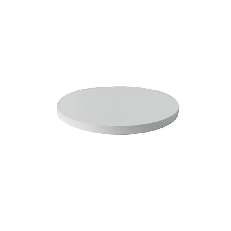
- High Dielectric Constant: Sc₂O₃ is known for its high dielectric constant, making it useful in capacitors and semiconductor devices.
- Thermal Stability: Sc₂O₃ maintains its properties even at elevated temperatures, making it suitable for harsh environments.
- Optical Transparency: Sc₂O₃ is transparent across a wide range of wavelengths, from UV to IR, which is beneficial in optical coatings and devices.
- Corrosion Resistance: Sc₂O₃ thin films are highly resistant to chemical corrosion, enhancing the longevity of coated surfaces.
-
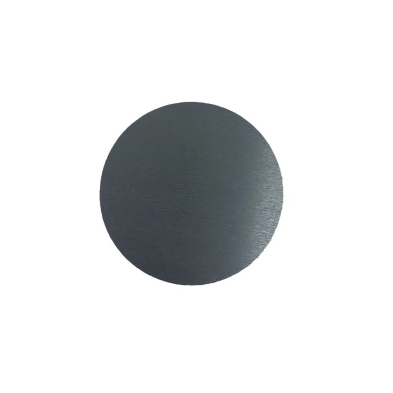
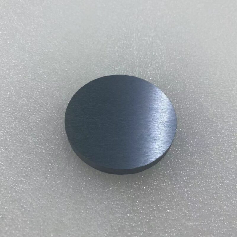
- Purity: High-purity selenium (typically 99.9% or higher) ensures the quality of the deposited films and consistent performance.
- Photoconductivity: Selenium is highly photoconductive, making it ideal for optoelectronic and photovoltaic applications.
- Customizable Size and Shape: Selenium sputtering targets are available in different forms, including discs, plates, and custom shapes, to fit a variety of PVD systems.
- Thermal and Electrical Properties: Selenium films offer excellent thermal and electrical properties, crucial for semiconductor and photovoltaic devices.
-
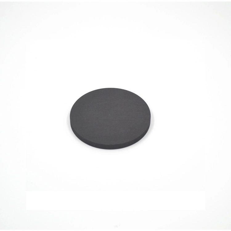
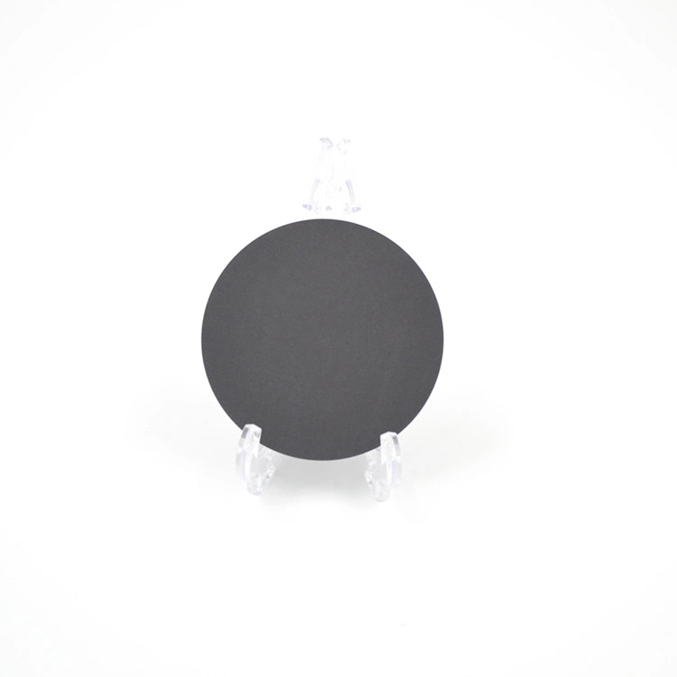
- Purity: Silicon sputtering targets are typically available in high purity (99.999% or higher) to ensure high-performance film deposition, particularly in sensitive semiconductor applications.
- Electrical Properties: Silicon is an intrinsic semiconductor, and thin films made from silicon offer excellent electrical characteristics for electronic and optoelectronic devices.
- Thermal Conductivity: Silicon’s thermal properties make it ideal for applications where heat dissipation is important, such as in power electronics and solar cells.
- Customizable Size and Shape: Silicon sputtering targets come in various forms, including discs, plates, and custom shapes to fit different deposition systems.
-
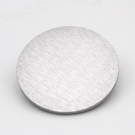
- High Purity: Ensures minimal contamination and consistent deposition performance.
- Optimal Stoichiometry: Precisely controlled Si and Te ratio for superior material properties.
- Wide Compatibility: Suitable for various deposition techniques, including PVD and sputtering.
- Excellent Film Properties: Supports the production of uniform, high-quality thin films.
- Customizable Options: Flexible sizes and shapes to fit diverse sputtering systems.