Showing 13–24 of 256 results
-

$51.00 – $96.00
- Ultra-high purity 5N (99.999%) for superior film uniformity and low defect density.
- Excellent sputtering performance with stable deposition rates.
- Low impurity levels meeting research-grade and semiconductor-grade requirements.
- Standard sizes in stock for fast delivery.
- Fully customizable in purity, diameter, thickness, and shape.
-
$80.00 – $105.00
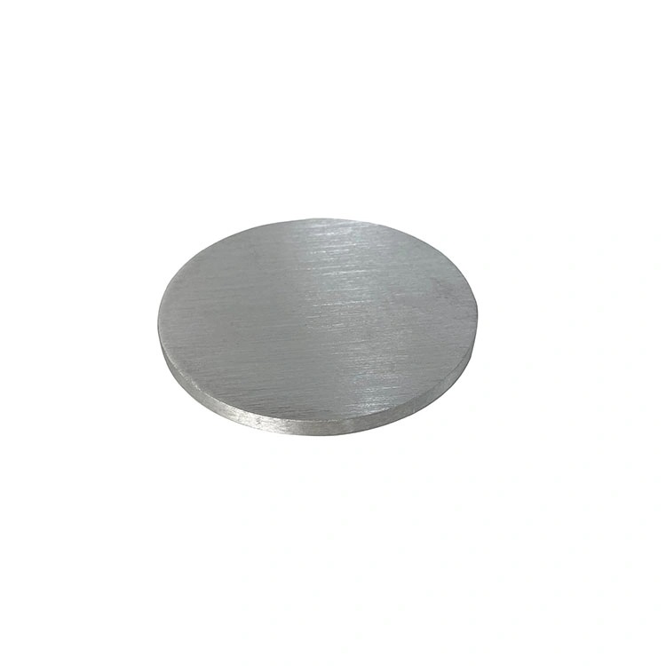
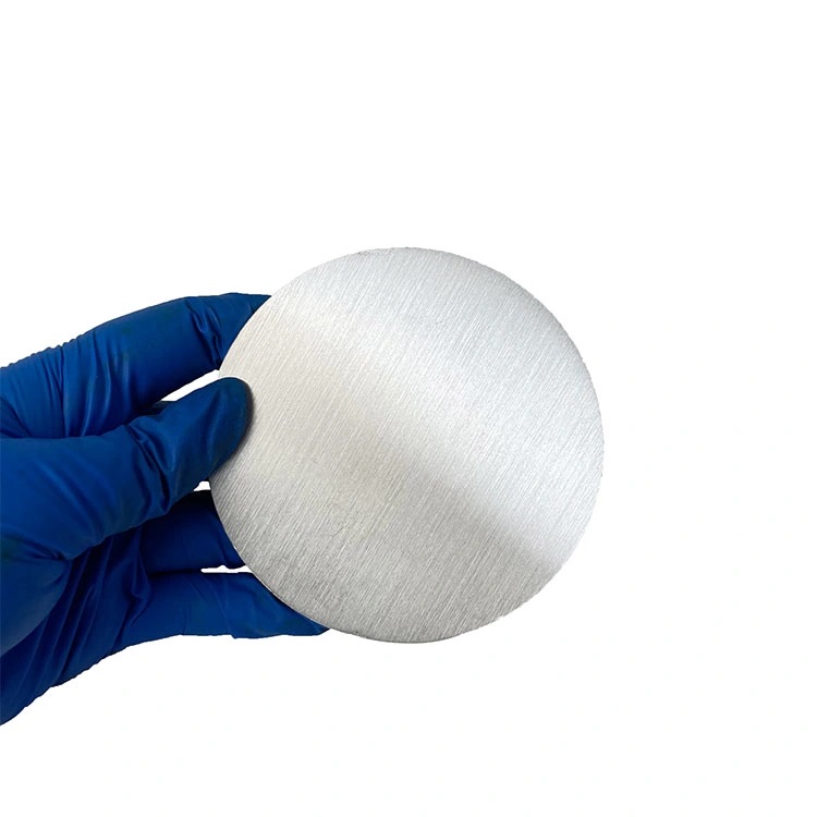
- Ultra-high purity 99.999% (5N), ensuring exceptional thin film quality and low impurity levels.
- Excellent sputtering performance, providing uniform film deposition and stable sputter rates.
- Multiple standard thickness options, including 6 mm with magnetic spacer for systems requiring enhanced magnetic coupling.
- High density and strong mechanical stability suitable for high-power sputtering systems.
- Customizable dimensions to match different sputtering equipment and process conditions.
-
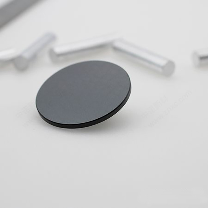
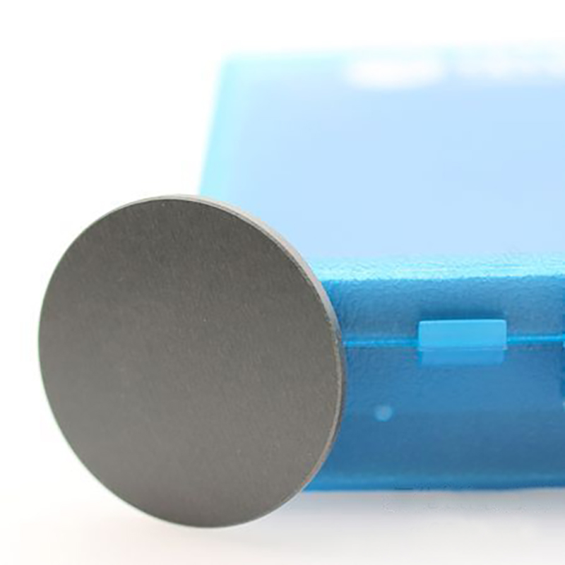
- High-purity ceramic target with excellent chemical composition consistency
- ZnO : Al₂O₃ = 98 : 2 wt% standard composition
- High density for stable sputtering performance
- Excellent electrical conductivity and optical transparency
- Uniform grain structure for consistent film deposition
- Low particle generation during sputtering
- High utilization efficiency and uniform erosion profile
- Suitable for both RF and DC magnetron sputtering systems
- Indium-free transparent conductive oxide material
- Custom sizes, purity levels, and backing plate bonding available
-
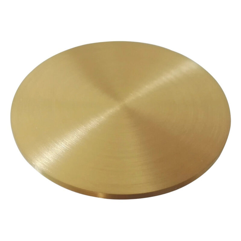
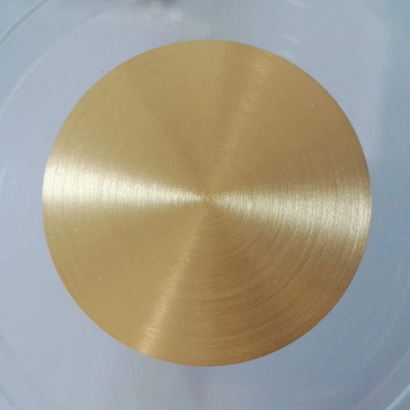
Gold (Au) sputtering target is a very important material of semiconductor, it’s used for depositing gold thin film on the surface of semiconductor chips, to form ohmic contact film, electrode or other films, it can form various metallic films system. Most of gold oxide film system can be used for manufacturing LED, microwave communication device, widely applied in spaceflight, aviation, semiconductor chips and Solar Cells.
-
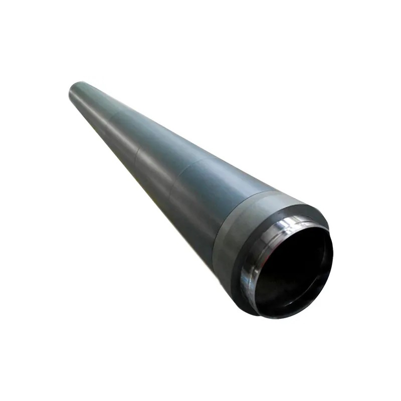
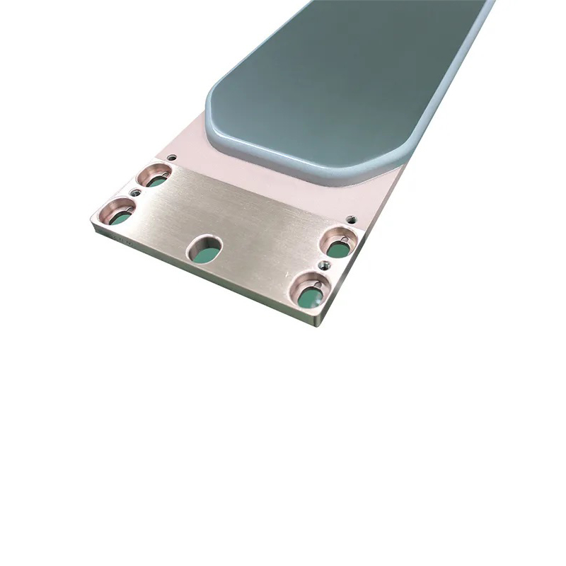
- High Optical Transparency: AZO offers excellent transparency in the visible spectrum, making it ideal for applications requiring clear conductive films.
- Good Electrical Conductivity: Despite its transparency, AZO provides high electrical conductivity, which is critical in photovoltaic cells and touchscreens.
- Environmentally Friendly: Unlike ITO, AZO does not rely on scarce or expensive elements like indium, making it a more sustainable and cost-effective choice.
- Thermal and Chemical Stability: AZO films maintain stability under various temperature and environmental conditions, making them suitable for outdoor and industrial applications.
- Low Reflectivity: AZO films are known for their low reflectance, which is beneficial in display technologies to reduce glare and improve visibility.
-
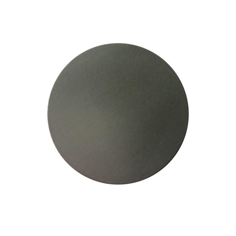

Boron (B) sputtering targets are high-purity materials used in physical vapor deposition (PVD) processes, particularly sputtering, to deposit thin films of boron onto various substrates. These targets are widely used in industries such as electronics, optics, and materials science due to boron’s unique properties.
-
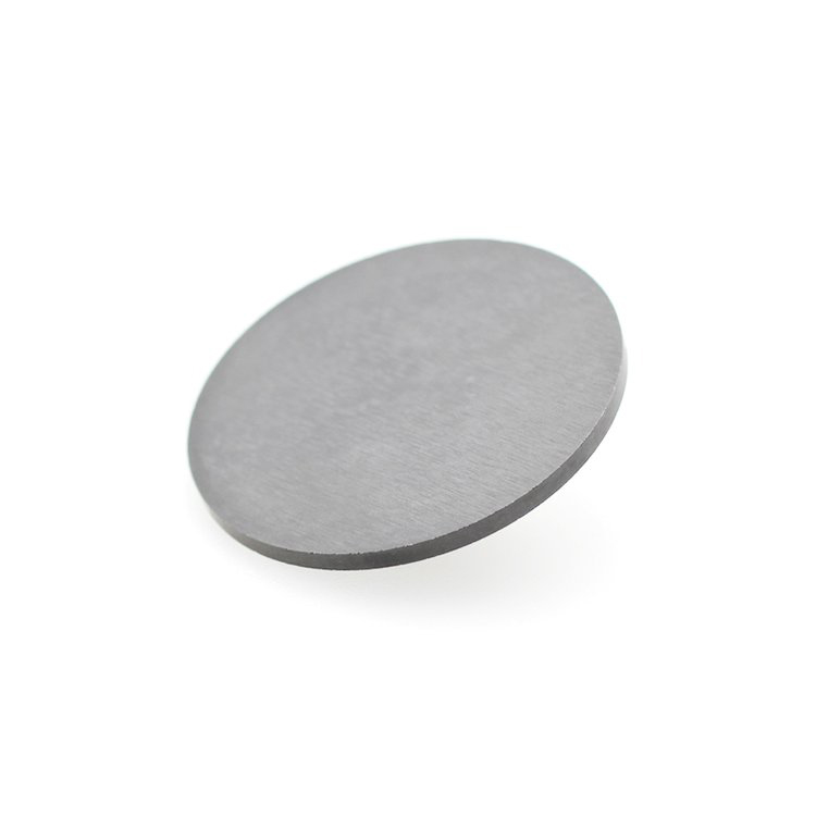
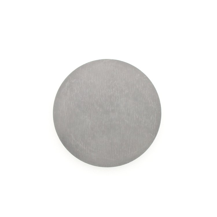
- Exceptional Hardness: High resistance to wear and abrasion.
- Chemical Stability: Resistant to acids and alkalis, ensuring longevity in extreme environments.
- Lightweight: Facilitates applications where low weight is critical.
- High Purity: Delivers superior film quality and consistency.
-
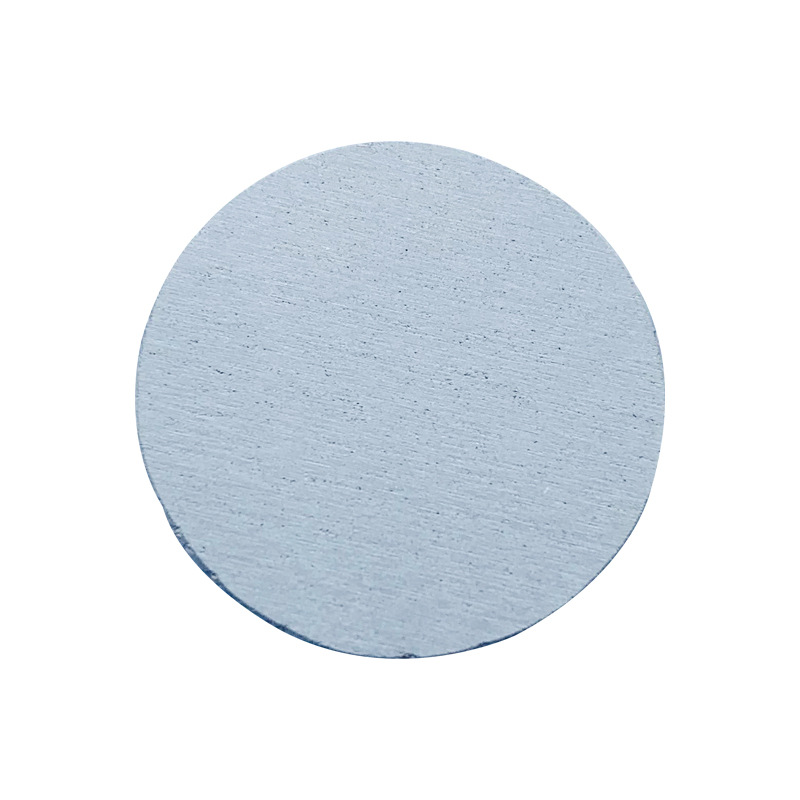
Barium (Ba) sputtering targets are high-purity materials used in physical vapor deposition (PVD) processes, particularly sputtering, to create thin films on various substrates. Barium targets are typically used in the production of optical coatings, semiconductor devices, and other advanced materials due to their unique properties.
-
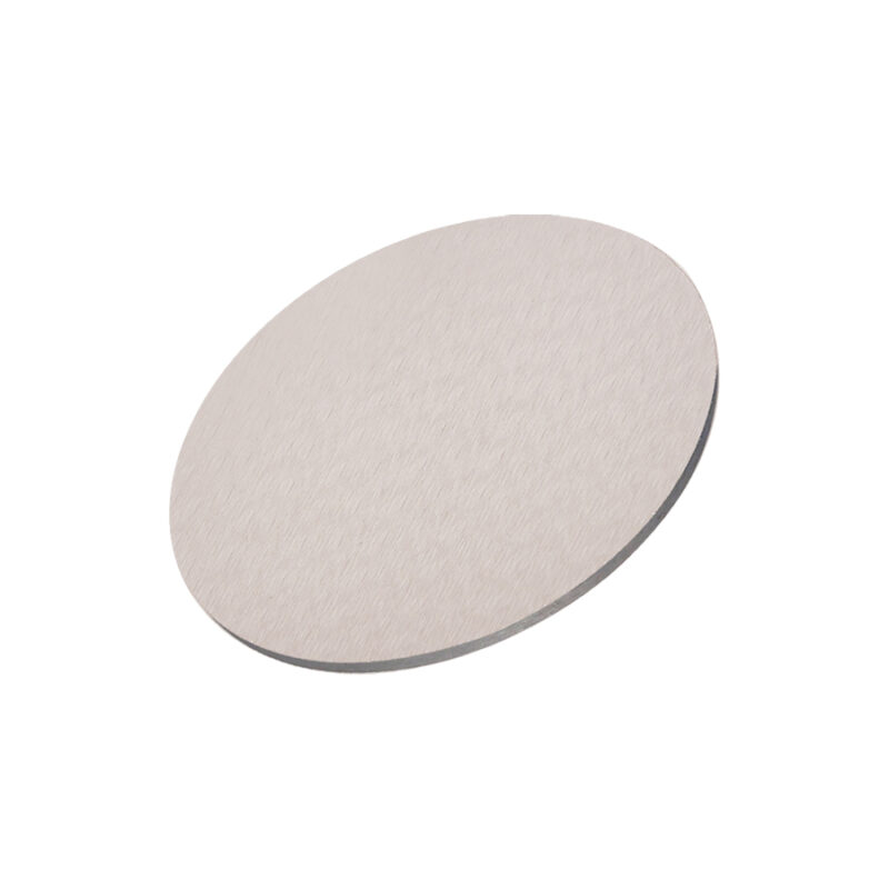
- High Dielectric Constant: BaTiO₃ is known for its exceptionally high dielectric constant, making it ideal for capacitors and electro-optic applications.
- Ferroelectric and Piezoelectric Properties: The material exhibits both ferroelectric and piezoelectric behaviors, making it suitable for memory devices, sensors, and actuators.
- Excellent Thermal Stability: BaTiO₃ maintains good thermal stability, ensuring reliable performance in high-temperature environments.
- High Purity and Low Defects: BaTiO₃ sputtering targets are available in high-purity grades (up to 99.999%), ensuring low defect densities in the deposited thin films, which is crucial for advanced electronic applications.
- Custom Composition: Barium Titanate can be tailored with dopants to modify its electrical and thermal properties, optimizing performance for specific applications.
-
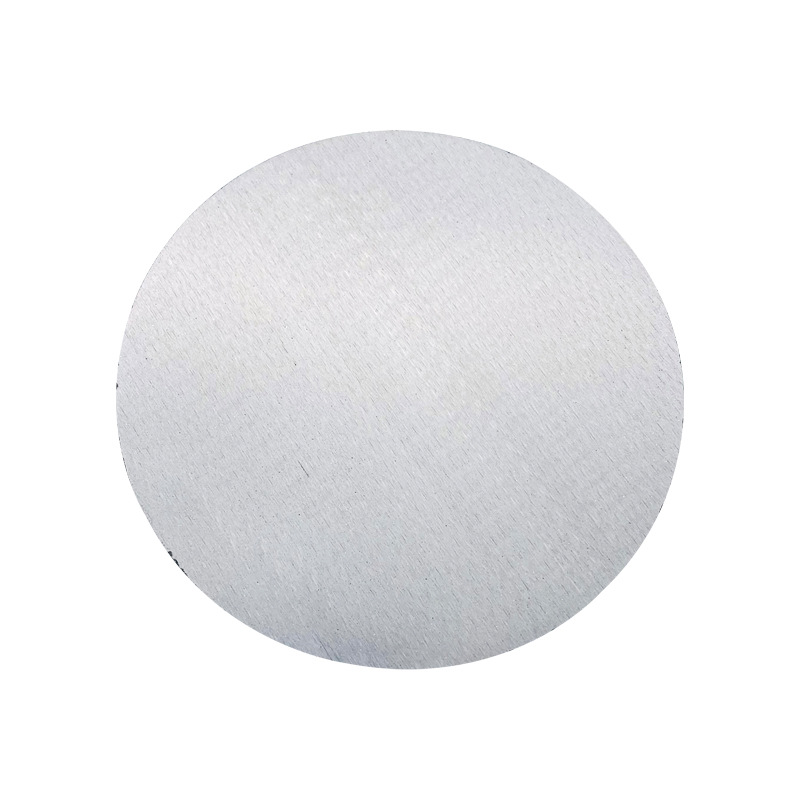
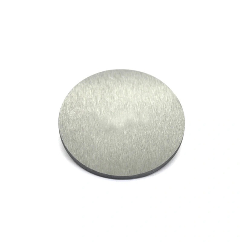
Bismuth (Bi) is a unique metal known for its low toxicity, high density, and distinct electronic properties, making it valuable in specific electronic, optical, and magnetic applications. Bismuth (Bi) sputtering targets are essential for industries requiring specialized thin films with unique electronic, optical, and magnetic properties, particularly in advanced electronics, superconductors, and optical devices.
-
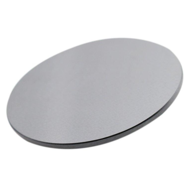
- Layered Structure: Enables the exfoliation of thin films for various nanodevice applications.
- High Carrier Mobility: Supports rapid electron and hole movement for faster electronic response.
- Tunable Bandgap: Adjustable for different applications, optimizing its use in various electronic and optical devices.
- Good Thermal Stability: Suitable for high-temperature applications, enhancing long-term reliability.
-
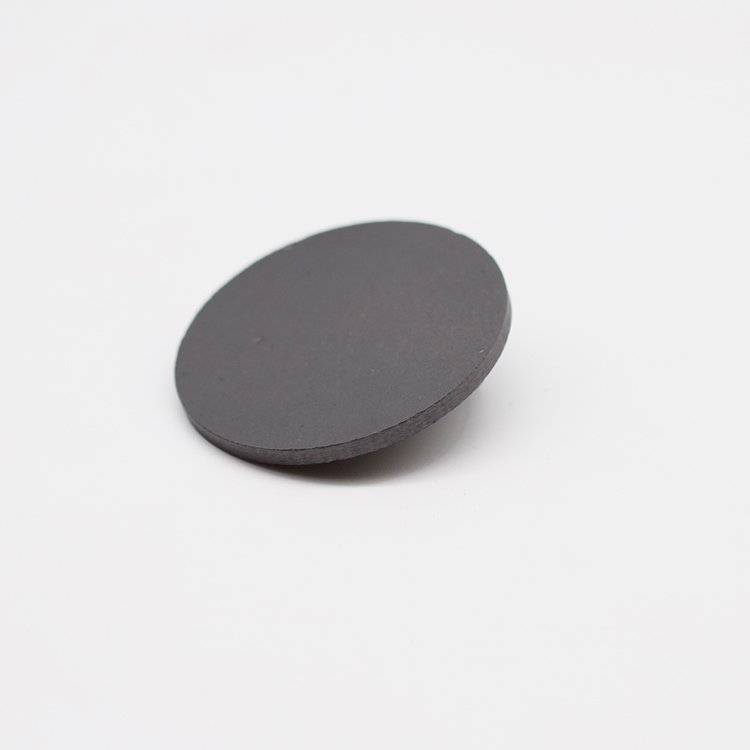
- High Conductivity: Bi₂S₃ films exhibit good electrical conductivity, making them ideal for use in electronic applications.
- Thermoelectric Efficiency: Known for its high thermoelectric performance, making it a key material in thermoelectric energy conversion devices.
- Optical Transparency: The material has desirable optical transparency in the visible spectrum, which is advantageous for optoelectronic applications.
- Chemical Stability: Bismuth Sulfide is stable under a wide range of chemical conditions, which ensures longevity and reliability in demanding environments.
- High Purity: Bi₂S₃ sputtering targets are available in high purity, ensuring the production of high-quality thin films with minimal contamination.